Light-emitting unit array, method for fabricating the same and projection apparatus

A technology of light-emitting units and projection equipment, applied in the direction of optical components, optical components, electrical components, etc.

Active Publication Date: 2012-02-01
IND TECH RES INST
View PDF9 Cites 34 Cited by
  • Summary
  • Abstract
  • Description
  • Claims
  • Application Information

AI Technical Summary

Problems solved by technology

An array of light-emitting ...

Method used


Image

  • Light-emitting unit array, method for fabricating the same and projection apparatus
  • Light-emitting unit array, method for fabricating the same and projection apparatus
  • Light-emitting unit array, method for fabricating the same and projection apparatus

Examples


no. 1 example

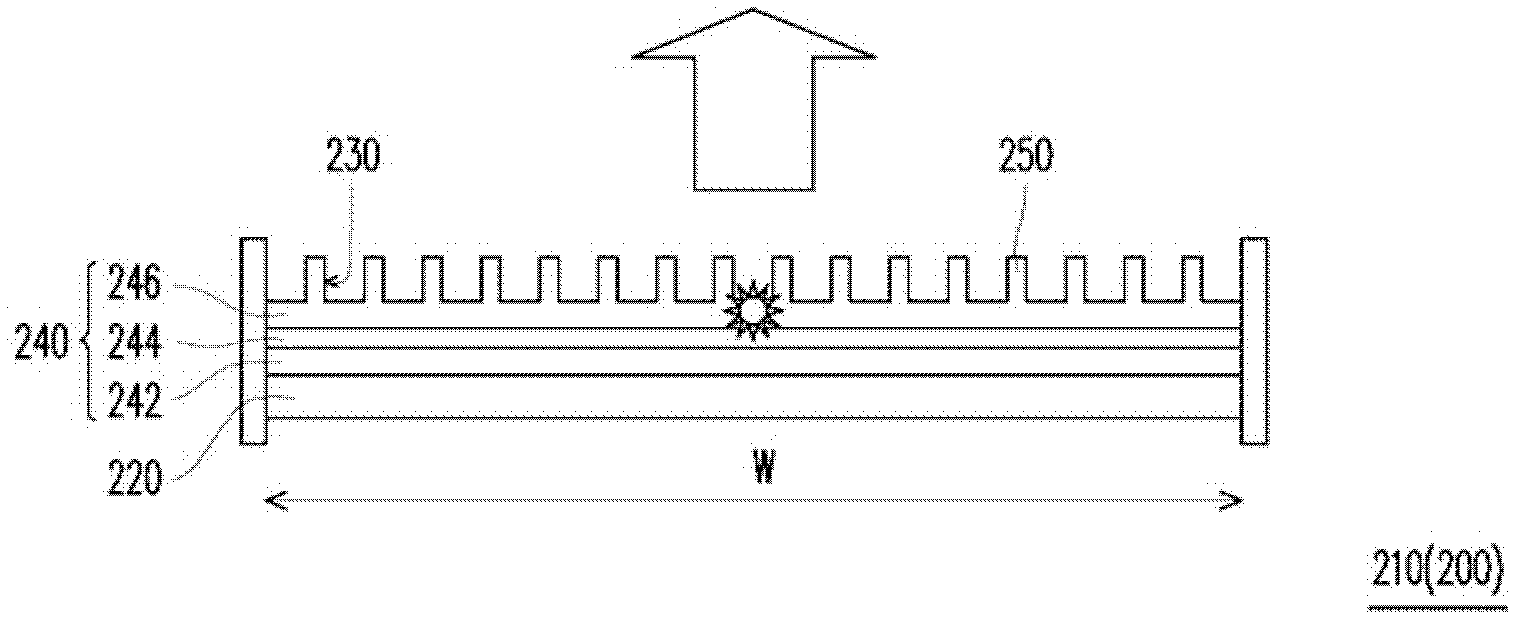
[0050] In this embodiment, a micro light-emitting diode (LED) array is realized by adjusting the thickness and structure of the epitaxial structure of the LED so as to optimize light extraction or light collimation to meet the requirements.

[0051] figure 1 is a schematic cross-sectional view of the micro LED array according to the first embodiment of the present invention. It should be noted that the micro LED array 200 has a plurality of micro LEDs arranged in an array and monolithically integrated, and for clarity of description, figure 1 Only the cross-sectional structure of one micro-LED in the micro-LED array is shown. see figure 1 , the micro LED 210 of the present embodiment comprises a reflective layer 220 and a light-emitting layer 240, wherein the light-emitting layer 240 comprises, for example, a P-type epitaxial layer 242, an N-type epitaxial layer 246, and a multiple quantum well sandwiched between these two epitaxial layers (multiple quantum well, MQW) 244 (...

no. 2 example

[0062] In this embodiment, the method of manufacturing a micro LED array is implemented by adding a sacrificial layer in specific steps and in specific positions of the micro LEDs, so as to simplify the overall manufacturing process of the micro LED array with higher light extraction and higher light collimation.

[0063] Figures 3A to 3E is a schematic cross-sectional view illustrating a process flow of a micro LED array according to a second embodiment of the present invention.

[0064] see Figure 3A , first provide a substrate 310 . The material of the substrate 310 is, for example, sapphire. In addition, the sacrificial layer 340 is added in the epitaxial stack layer intended to form the micro-LED structure, so that the micro-LED 300 can easily achieve the desired thickness of the micro-cavity resonance. More specifically, the undoped gallium nitride (un-GaN) layer 320, the first n-type doped gallium nitride (n-GaN) layer 330, the sacrificial layer 340, the second n-G...

no. 3 example

[0076] In this present embodiment, a micro-LED array is implemented for tuning the external field distribution of the micro-LEDs in order to optimize light extraction and light collimation to meet requirements. In some embodiments, the micro LED array can also reduce cross-talking.

[0077] Figures 5A to 5D is a schematic cross-sectional view illustrating a process flow of a micro-optical lens structure of a micro-LED array according to a third embodiment of the present invention, wherein the micro-LED array in this embodiment further includes a micro-optical lens structure, and LEDs are correspondingly disposed therein . For better illustration, Figures 5A to 5D Only the micro-optical lens structure is shown, and the micro-LED disposed therein is omitted. The micro LED array can be any of the micro LED arrays mentioned above or any other kind of micro LED array, this embodiment is not limited in terms of the type of micro LED array.

[0078] see Figure 5A , forming th...


PUM


Abstract

A projection apparatus (1200) is provided. The projection apparatus (1200) includes a light-emitting unit array (1210), an optical sensor (1230), and a control unit (1220). The light-emitting unit array (1210) is for emitting an image beam projected onto a screen (60). The optical sensor (1230) is for detecting electromagnetic waves from at least one of the screen (60) and an environment (70) so as to generate a signal. The control unit (1220) is electrically coupled to the light-emitting unit array (1210) and the optical sensor (1230) for controlling emission of the light-emitting unit array (1210) according to the signal from the optical sensor (1230). A light-emitting unit array (1210) and a method for fabricating a light-emitting unit array (1210) are also provided.

Description

technical field [0001] The present invention relates to a light emitting diode (light emitting diode, LED) array and a manufacturing method thereof, and to a display device, and more particularly to a method capable of enhancing light extraction (light extraction) efficiency and collimation (collimation) A light-emitting unit array, a manufacturing method thereof, and a projection device. Background technique [0002] In recent years, light-emitting diodes (LEDs) have gradually improved luminous efficiency and replaced fluorescent and incandescent lamps in some fields, including highly responsive speed lamps for scanners, backlights for liquid crystal displays (LCDs) (backlight source) or front light source (front light source), light source for instrument panel of automobile, traffic signal light, light source for projection device and even general lighting device. The light emission of LEDs is usually cold light emission, rather than through heat or discharge, so LEDs oft...

Claims


Application Information

Patent Timeline
IPC IPC(8): G02B27/18H01L33/00
CPCG03B21/00H01L2933/0083H01L33/504H01L33/60H04N9/315H01L27/156G03B21/005
Inventor 叶文勇赵嘉信庄育洪黎家伶赖俊峰颜玺轩戴晟杰戴光佑陈泽澎
Owner IND TECH RES INST
Why Eureka
Try Eureka