System for plasma process

A plasma and process technology, which is applied in the field of semiconductor process systems, can solve problems such as complexity and particle pollution, and achieve the effect of improving particle conditions and increasing yield

Active Publication Date: 2014-03-19
SEMICON MFG INT (SHANGHAI) CORP +1
View PDF6 Cites 0 Cited by
  • Summary
  • Abstract
  • Description
  • Claims
  • Application Information

AI Technical Summary

Problems solved by technology

[0008] Although the above two methods can reduce the presence of particles in the plasma reaction chamber, in practice, there are still particles contaminating the wafer and each chamber of the machine.
In addition, the above solutions are more complicated to implement and have certain costs

Method used


Image

  • System for plasma process

Examples


Embodiment Construction

[0018] In the following description, numerous specific details are given in order to provide a more thorough understanding of the present invention. It will be apparent, however, to one skilled in the art that the present invention may be practiced without one or more of these details. In other examples, some technical features known in the art are not described in order to avoid confusion with the present invention.

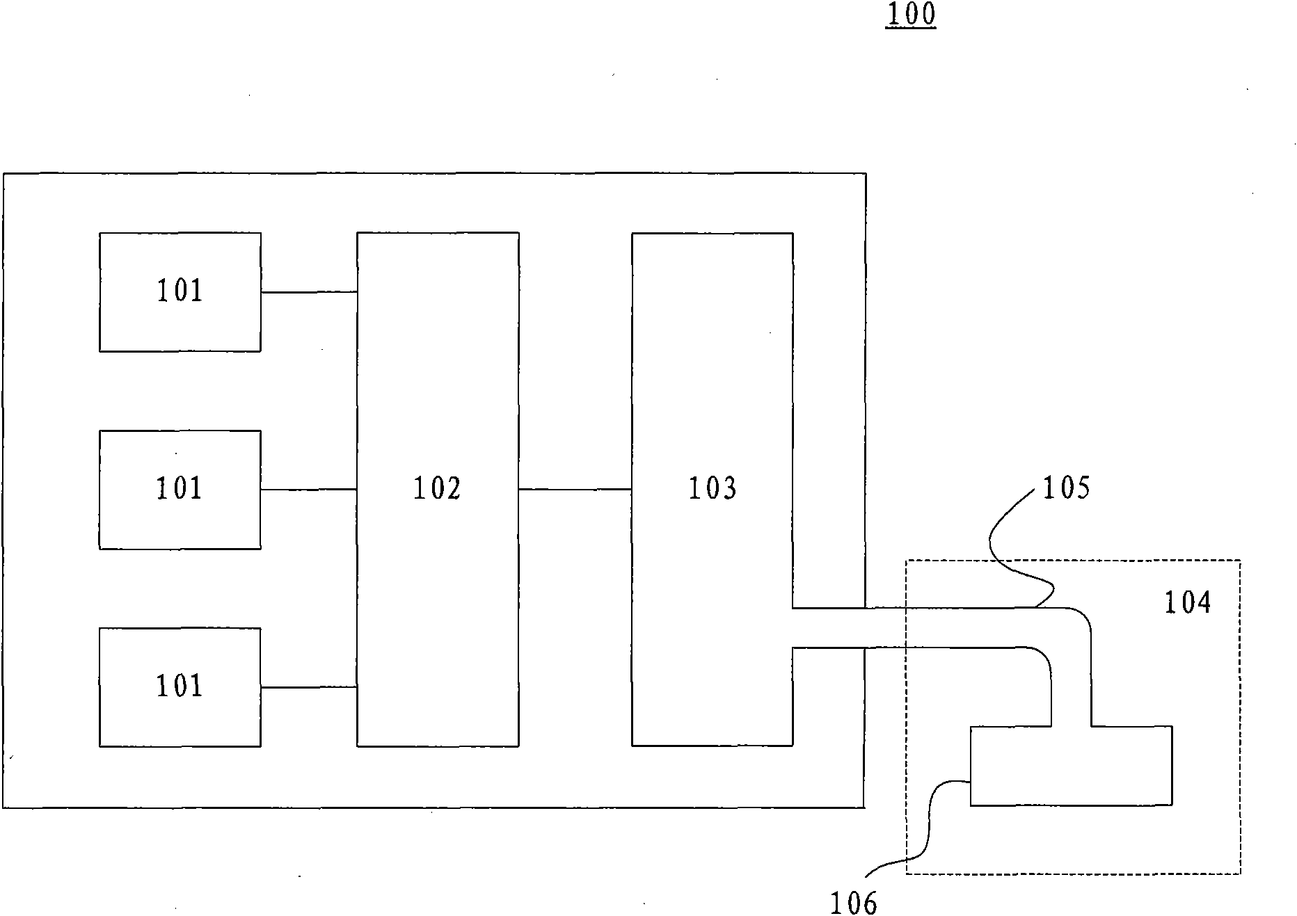
[0019] In the prior art, improvements are only made to the cleaning and cleaning of the plasma reaction chamber, but the problems in the prior art are also related to the vacuum transfer chamber and the atmospheric transfer chamber. Specifically, the dust existing in the plasma reaction chamber will also diffuse into the above-mentioned vacuum transfer chamber and atmospheric transfer chamber while the wafer is being transferred. On the other hand, vacuum transfer chambers and atmospheric transfer chambers themselves are also a source of particles and dust. Su...


PUM


Abstract

The invention discloses a system for a plasma process. The system comprises an atmosphere transmission cavity, a vacuum transmission cavity, a plasma reaction cavity and at least one air exhaust device, wherein the vacuum transmission cavity is connected between the plasma reaction cavity and the atmosphere transmission cavity; one end of the air exhaust device is connected to the atmosphere transmission cavity; and the air exhaust device is used for exhausting air from the atmosphere transmission cavity to the exterior of the system. The system can improve the particle condition in the plasma process and increase the yield rate.

Description

technical field [0001] The invention relates to a semiconductor process system, in particular to a system used in plasma process. Background technique [0002] Plasma etching in the semiconductor process is one of the key processes in the manufacture of integrated circuits, and is widely used in the manufacture of microprocessors (CPUs), memories and various logic circuits. Its purpose is to completely copy the mask pattern to the surface of the semiconductor wafer. Plasma etching has the characteristics of good selectivity, less damage to the substrate, and good anisotropy. The principle of plasma etching of wafers is: under low pressure, the process gas is excited by radio frequency power to generate ionization and form plasma. The plasma is composed of charged electrons and ions. The process gas in the etching chamber is in the Under the impact of electrons, in addition to transforming into ions, it can also absorb energy and form a large number of active groups; the ac...

Claims


Application Information

Patent Timeline
Patent Type & Authority Patents(China)
IPC IPC(8): H01L21/00H01L21/3065H01J37/32
Inventor 陆东张建
Owner SEMICON MFG INT (SHANGHAI) CORP
Why Eureka
Try Eureka