LED (light-emitting diode) packaging method and LED packaging structure
A technology of LED encapsulation and encapsulation method, which is applied in the direction of electrical components, electric solid devices, circuits, etc., can solve the problems of cumbersome preparation process and complex substrate structure, and achieve the effects of simple substrate structure, prolonging the service life of LEDs, and good heat dissipation performance
- Summary
- Abstract
- Description
- Claims
- Application Information
AI Technical Summary
Problems solved by technology
Method used
Image

Examples
Embodiment Construction
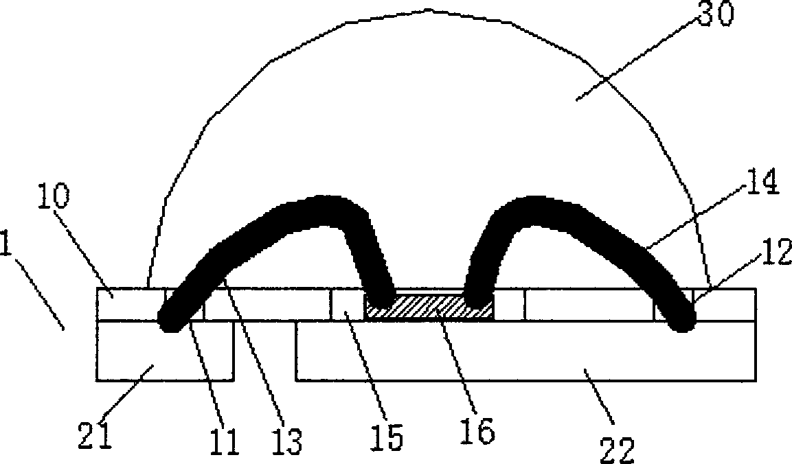
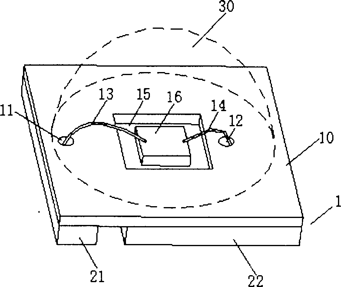
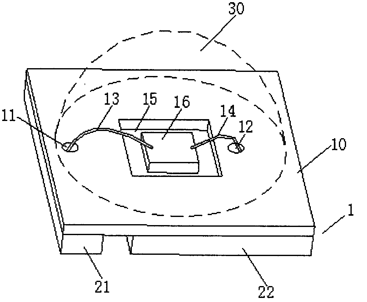
[0027] The packaging method of the LED adopts a new substrate, the substrate uses an insulating base material as an insulating layer, and two copper substrates are pasted at intervals on the lower end of the insulating layer, and corresponding circuits and electrodes are respectively formed on it, wherein The size of one copper substrate is larger than that of the other copper substrate, the positive electrode is formed on the large-sized copper substrate, and the negative electrode is formed on the small-sized copper substrate. An LED chip installation groove is provided on the insulating layer, and the LED chip installation groove is located at the insulating layer where the large-size copper substrate is stacked. The LED chip installation groove is set through the insulating layer, and the LED chip is placed on the exposed copper substrate at the bottom of the LED chip installation groove, so that the LED chip is placed in the LED chip installation groove. Two through holes...
PUM
 Abstract
Description
Claims
Application Information
 - Generate Ideas
- Intellectual Property
- Life Sciences
- Materials
- Tech Scout
- Unparalleled Data Quality
- Higher Quality Content
- 60% Fewer Hallucinations
Browse by: Latest US Patents, China's latest patents, Technical Efficacy Thesaurus, Application Domain, Technology Topic, Popular Technical Reports.
© 2025 PatSnap. All rights reserved.Legal|Privacy policy|Modern Slavery Act Transparency Statement|Sitemap|About US| Contact US: help@patsnap.com