Highly miniaturized substrate integrated waveguide resonator

A substrate integrated waveguide and resonator technology, applied in the direction of resonators, waveguide devices, electrical components, etc., can solve the problems of large volume, unfavorable system miniaturization design, and difficulty in reducing circuit size, etc., to reduce the circuit area , good out-of-band suppression ability, reduce the effect of mutual coupling and crosstalk

Inactive Publication Date: 2012-02-15
UNIV OF ELECTRONICS SCI & TECH OF CHINA
View PDF6 Cites 26 Cited by
  • Summary
  • Abstract
  • Description
  • Claims
  • Application Information

AI Technical Summary

Problems solved by technology

[0004] However, the existing substrate-integrated waveguide resonators also inherit a major disadvantage of metal waveguide resonators, that is, larger volume
Compared with traditional planar resonators composed o

Method used


Image

  • Highly miniaturized substrate integrated waveguide resonator
  • Highly miniaturized substrate integrated waveguide resonator
  • Highly miniaturized substrate integrated waveguide resonator

Examples


Embodiment 1

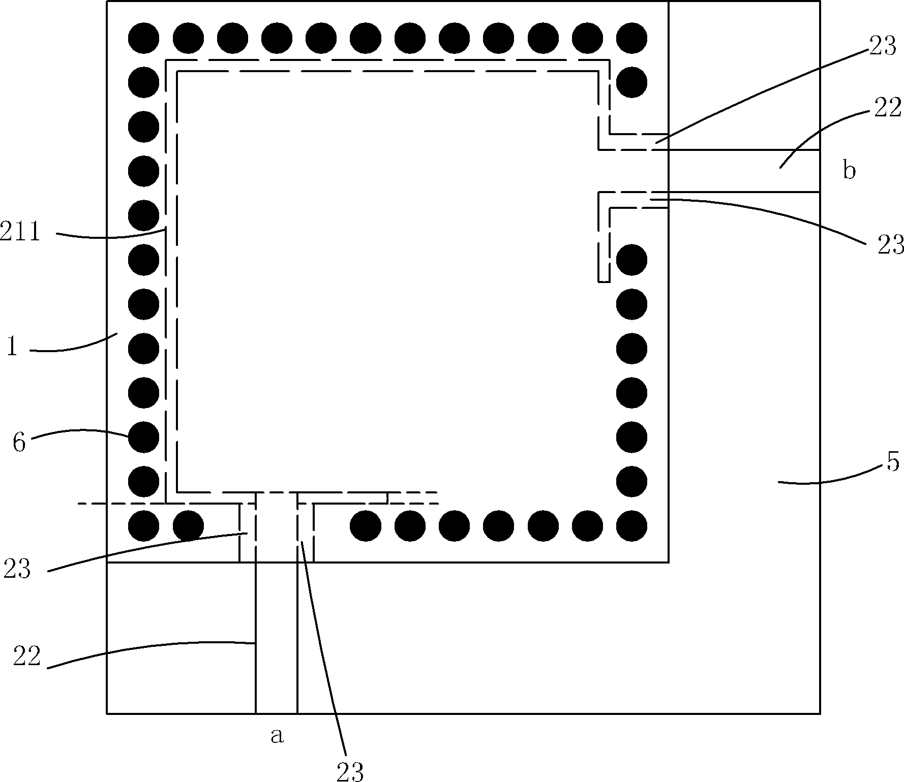
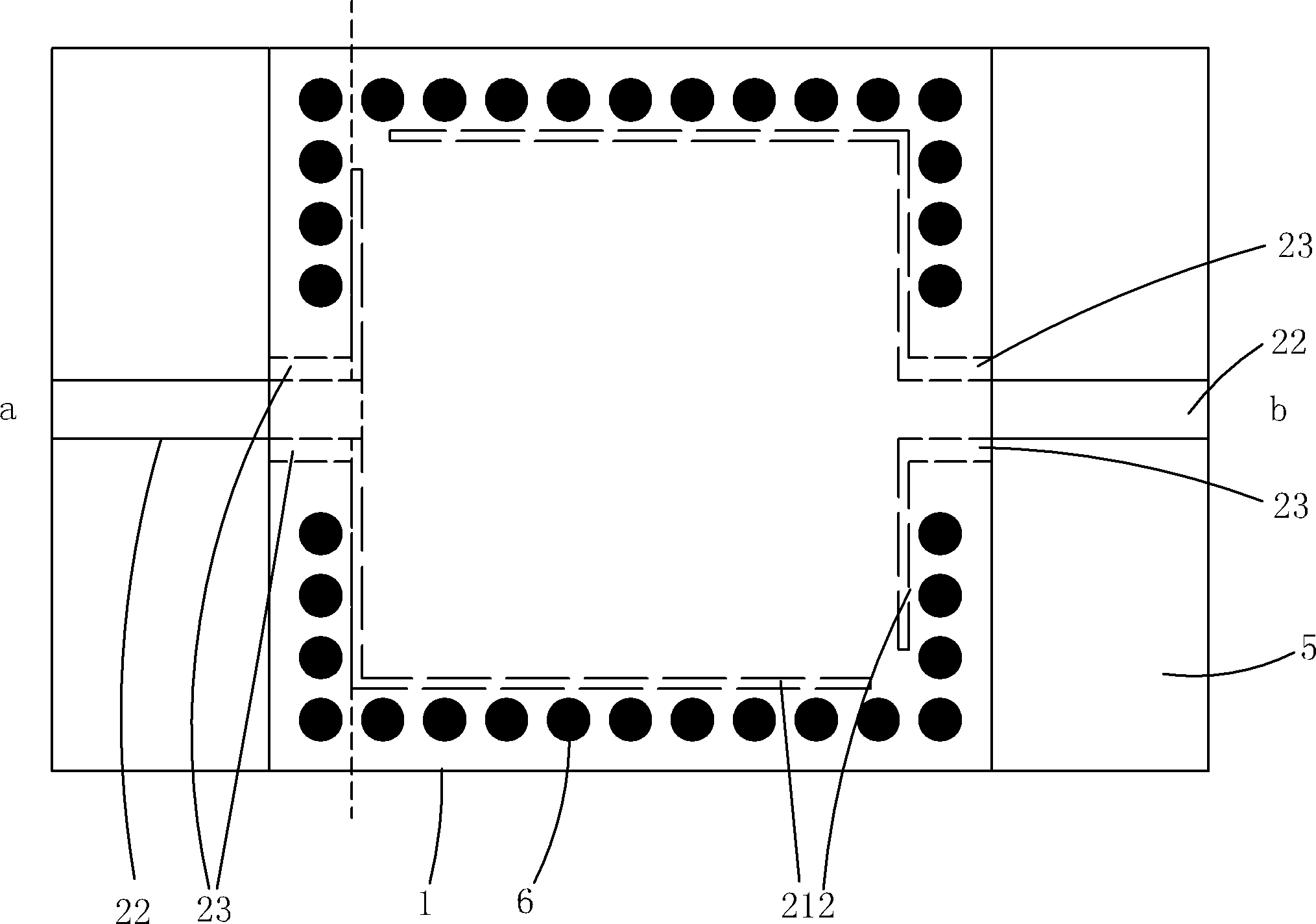
[0021] Embodiment 1: as figure 1 , figure 2 As shown, a highly miniaturized substrate-integrated waveguide resonator includes a first metal copper-clad layer 1, a first dielectric layer 4, a second metal copper-clad layer 2, and a second dielectric layer stacked sequentially from top to bottom. 5 and the third metal copper clad layer 3, in order to form the highly miniaturized substrate integrated waveguide resonator of the present invention, the second metal copper clad layer 2 is processed to form the required metal pattern ( Circuit structure), the first metal copper clad layer 1 and the third metal copper clad layer 3 are not processed, and the parts in the pattern are divided by imaginary short dashed lines, and the metallized through holes 6 pass through the first metal clad layer in turn. The copper layer 1, the first dielectric layer 4, the second metal copper clad layer 2, the second dielectric layer 5 and the third metal copper clad layer 3 are connected to form tw...

Embodiment 2

[0024] Embodiment 2: as figure 1 , image 3 As shown, a highly miniaturized substrate-integrated waveguide resonator includes a first metal copper-clad layer 1, a first dielectric layer 4, a second metal copper-clad layer 2, and a second dielectric layer stacked sequentially from top to bottom. 5 and the third metal copper clad layer 3, in order to form the highly miniaturized substrate integrated waveguide resonator of the present invention, the second metal copper clad layer 2 is processed to form the required metal pattern ( circuit structure), the first metal copper-clad layer 1 and the third metal copper-clad layer 3 are not treated, the parts in the pattern are divided by imaginary short dashed lines, and the metallized through holes 6 pass through the first The metal copper clad layer 1, the first dielectric layer 4, the second metal copper clad layer 2, the second dielectric layer 5 and the third metal copper clad layer 3 are connected to form two stacked square cavit...

Embodiment 3

[0027] Embodiment 3: as figure 1 , Figure 4 As shown, a highly miniaturized substrate-integrated waveguide resonator includes a first metal copper-clad layer 1, a first dielectric layer 4, a second metal copper-clad layer 2, and a second dielectric layer stacked sequentially from top to bottom. 5 and the third metal copper clad layer 3, in order to form the highly miniaturized substrate integrated waveguide resonator of the present invention, the second metal copper clad layer 2 is processed to form the required metal pattern ( circuit structure), the first metal copper-clad layer 1 and the third metal copper-clad layer 3 are not treated, the parts in the pattern are divided by imaginary short dashed lines, and the metallized through holes 6 pass through the first The metal copper-clad layer 1, the first dielectric layer 4, the second metal copper-clad layer 2, the second dielectric layer 5 and the third metal copper-clad layer 3 are connected to form two sets of stacked iso...


PUM

PropertyMeasurementUnit
Thicknessaaaaaaaaaa

Abstract

The invention relates to a highly miniaturized substrate integrated waveguide resonator which comprises a first metal copper-coated layer, a first medium layer, a second metal copper-coated layer, a second medium layer and a third metal copper-coated layer which are successively overlaid from top to bottom, wherein a metalizing through hole is connected with the third metal copper-coated layer after successively penetrating through the above interlayer to form an upper group of overlaid square cavities and a lower group of overlaid square cavities; in the second metal copper-coated layer, one group of C-shaped slots penetrating through the second metal copper-coated layer is arranged close to the metalizing through hole corresponding to the position of the square cavities; two microstrip lines are respectively connected close to two ends of the C-shaped slots; two sides of the microstrip line, which are close to one ends of the C-shaped slots, are respectively provided with a coupling slot penetrating through the second metal copper-coated layer; the coupling slot is connected with the C-shaped slots; and the metalizing through hole is broken on the positions of the microstrip lines and the coupling slots. The high-density miniaturized substrate integrated waveguide resonator has the beneficial effect that the traditional substrate integrated waveguide resonator structure is folded so as to greatly reduce the circuit area of the existing resonator, and highly miniaturization is realized.

Description

technical field [0001] The invention belongs to the technical field of microwave and millimeter wave passive devices, in particular to a substrate integrated waveguide resonator in microwave and millimeter wave passive devices. Background technique [0002] In order to meet the development requirements of modern communication technology, one of the development trends of microwave and millimeter wave circuits and systems is miniaturization. The miniaturization of the system is based on the miniaturization of a single component, so the miniaturization of a single microwave device is one of the key issues to be solved in circuit design. [0003] Resonators are the basis of microwave circuits and are widely used in the design of filters, oscillators and other circuits. According to the requirements of the overall circuit of the system, the resonator can be realized by structures such as microstrip lines and metal waveguides, or by a substrate integrated waveguide structure that...

Claims


Application Information

Patent Timeline
IPC IPC(8): H01P7/00
Inventor 程钰间张传安樊勇
Owner UNIV OF ELECTRONICS SCI & TECH OF CHINA
Why Eureka
Try Eureka