New method for synthesizing patterned single-crystal tungsten oxide nanowire arrays with catalyst localization technology

A tungsten oxide nanowire, patterning technology, applied in gaseous chemical plating, metal material coating process, coating and other directions, can solve the problems of poor morphology and structure controllability, high reaction temperature, high production cost, etc. Achieving the effect of high field emission uniformity

Active Publication Date: 2012-02-22
SUN YAT SEN UNIV
View PDF2 Cites 24 Cited by
  • Summary
  • Abstract
  • Description
  • Claims
  • Application Information

AI Technical Summary

Problems solved by technology

[0005] The preparation methods listed above, or use liquid phase method to prepare tungsten oxide nanowires in solution, or prepare tungsten oxide one-dimensional nanomaterials by high temperature evaporation method or chemical vapor deposition method, the products obtained by these technologies are disordered tungsten oxide Most of them are nanowires, and the reaction temperature is high (>800°C), and the controllability of the shape and structure is poor. At the same time, a product mixed with tungsten oxide nanostructures of different phases is often obtained, and the production cost is relatively expensive, and the physical properties of the product are poor. , and the field emission performance cannot meet the needs of device applications. The most important thing is that the low-temperature (<550°C) localized preparation of patterned tungsten oxide nanostructure films cannot be realized, so it is largely restricted in the field of micro-nano electronic devices. the rapid development of

Method used


Image

  • New method for synthesizing patterned single-crystal tungsten oxide nanowire arrays with catalyst localization technology
  • New method for synthesizing patterned single-crystal tungsten oxide nanowire arrays with catalyst localization technology
  • New method for synthesizing patterned single-crystal tungsten oxide nanowire arrays with catalyst localization technology

Examples


Embodiment 1

[0043] Example 1: Preparation of patterned single crystal W0 by catalyst localization technology at low temperature 2 nanowire array

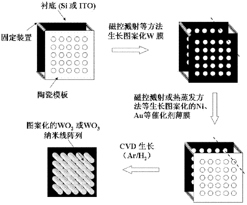
[0044] Using magnetron sputtering technology, using self-made ceramic template device or exposure technology of micro-processing technology, firstly, in the environment of Ar gas, the sputtering power is 300W, the sputtering time is 30min, and a layer of W with a thickness of about 400nm is grown. film, and then sputter-grow a layer of Ni nanoparticle film with a thickness of about 5 nm patterned on the W film.

[0045] The samples with W film and patterned Ni nanoparticle film grown sequentially were put into the CVD system, and the temperature was raised to 400 °C under the protection of Ar gas, and the 2 Insulated in an atmosphere of Ar gas for 1 h, then rapidly heated to 450 °C under the protection of Ar gas, and the growth pressure was 400 Pa. After 2 h of heat preservation, patterned WO was grown on the Si substrate. 2 array of nanowire...

Embodiment 2

[0047] Example 2: Preparation of patterned single crystal WO by catalyst localization technology at low temperature 3 nanowire array

[0048] Using magnetron sputtering technology, using self-made ceramic template device or exposure technology of micro-processing technology, firstly, in the environment of Ar gas, the sputtering power is 300W, the sputtering time is 30min, and a layer of W film with a thickness of about 400nm is grown. , and then a patterned Au nanoparticle film with a thickness of about 3 nm was vacuum evaporated on top of the W film.

[0049] The samples with W thin film and patterned Au nanoparticle thin film grown sequentially were placed in the CVD system, and the temperature was raised to 500 °C under the protection of Ar gas. 2 Insulated in an atmosphere of Ar gas for 1 h, then rapidly heated to 550 °C under the protection of Ar gas, the growth pressure was 8000 Pa, and after 2 h of growth, patterned WO could be grown on the Si substrate. 3 array of na...

Embodiment 3

[0051] Example 3: Using Catalyst Localization Technology to Prepare WO at Different Growth Temperatures 2 Nanowires

[0052] Keeping the argon (Ar) carrier gas flow rate as 200sccm, the reaction pressure as 400Pa, and the reaction time of 2h under the reaction conditions, change the reaction temperature to prepare WO 2 Nanowire array:

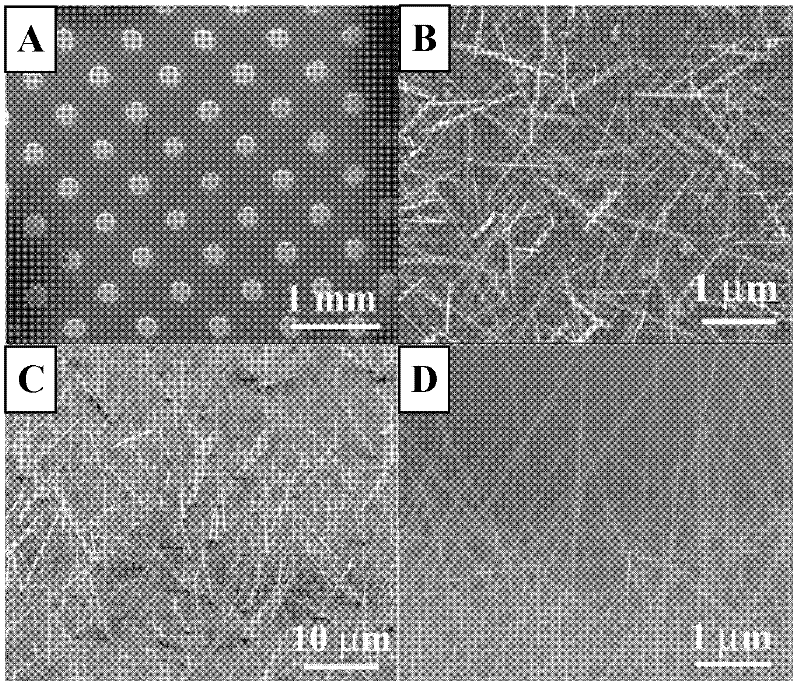
[0053] (1) When the reaction temperature is 550 °C, a higher density WO can be prepared on the Si substrate 2 The nanowire has a length of 2-3μm and a diameter of 40nm, and the shape and diameter of the nanowire are relatively uniform, such as Figure 8 As shown in A

[0054] (2) When the reaction temperature is 600°C, WO 2 The density of the nanowires decreased while the diameter increased to about 60nm, as shown in Figure 8 Shown in B.

[0055] (3) When the reaction temperature is 700°C, WO 2 The diameter of the nanowire increases significantly, and the diameter distribution range is large. Between 40-100nm, the density of the nanowir...


PUM

PropertyMeasurementUnit
thicknessaaaaaaaaaa
lengthaaaaaaaaaa
diameteraaaaaaaaaa

Abstract

The invention discloses a new method for synthesizing patterned single-crystal tungsten oxide nanowire arrays with a catalyst localization technology. Employing a tungsten film as a source material and a metal nanoparticle film as a catalyst, the method comprises: (a) catalyst film localization synthesis: realizing film patterning through fixation of a ceramic template and a substrate material together or application of the exposure technology in a micromachining process, then enabling localization growth of the catalyst nanoparticle film in a vacuum plating instrument; (b) chemical vapor deposition: in a reaction gas atmosphere and at a temperature of 400-800DEG C, placing a W film into a CVD device for growth of 1-8h, then opening a fixation device or removing a photoresist, thus finally obtaining patterned tungsten oxide nanowire arrays. The preparation method of the invention not only can prepare patterned tungsten oxide nanowire arrays of different growth density, but also has the advantages of low reaction temperature (lower than 500DEG C) and suitability for the growth of low-melting point substrates.

Description

technical field [0001] The invention relates to a new method for synthesizing a patterned tungsten oxide nanowire array by using catalyst localization technology, in particular to a method for preparing patterned tungsten oxide nanowire array thin film by using catalyst thin film localization technology combined with chemical vapor deposition technology. Background technique [0002] Since the first discovery of carbon nanotubes by Iijima in 1991, one-dimensional nanomaterials have attracted extensive attention due to their more unique physical and chemical properties compared with their bulk materials. In the 21st century, when the micro-nano electronics industry is booming, the preparation and physical characteristics of nano-devices based on one-dimensional nano-material arrays have become the focus of the world's scientific and technological circles. As we all know, Piezoelectric (Piezoelectric) devices, Field Electron Emission Display (FED) devices, Gas Sensors (Gas Sen...

Claims


Application Information

Patent Timeline
Patent Type & Authority Applications(China)
IPC IPC(8): C23C16/40C23C16/04C23C16/02C23C16/56
Inventor 许宁生刘飞李力邓少芝陈军
Owner SUN YAT SEN UNIV
Why Eureka
Try Eureka