Laser optical fiber coupling device containing non-imaging optical element

A fiber coupling device and non-imaging optics technology, applied in the coupling direction of optical waveguide, can solve the problems of poor illumination uniformity, alternating light and dark stripes, high cost, and uneven spot, so as to reduce damage to laser tubes and optical fibers The probability of high yield, the effect of improving the yield and the simple adjustment process

Inactive Publication Date: 2012-03-07
CHANGCHUN INST OF OPTICS FINE MECHANICS & PHYSICS CHINESE ACAD OF SCI
View PDF3 Cites 3 Cited by
  • Summary
  • Abstract
  • Description
  • Claims
  • Application Information

AI Technical Summary

Problems solved by technology

[0004] In order to solve the disadvantages of poor lighting uniformity, uneven light spots, bright and dark stripes and high cost in the prior art, the purpose of the present invention is to provide a laser fiber coupling device containing non-imaging optical elements, and its technical solution can solve Problems with Existing Technology

Method used


Image

  • Laser optical fiber coupling device containing non-imaging optical element
  • Laser optical fiber coupling device containing non-imaging optical element
  • Laser optical fiber coupling device containing non-imaging optical element

Examples


Embodiment Construction

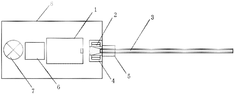
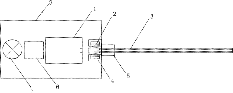
[0010] Depend on figure 1 As shown, a laser fiber coupling device containing non-imaging optical elements, the light source includes: a semiconductor laser tube 1, a non-imaging condenser lens 2 and an optical fiber 3, the semiconductor laser tube 1 emits a beam, and the beam passes through the non-imaging condenser lens 2 , converge on the rear surface of the non-imaging condenser lens 2, and then the beam enters the optical fiber 3 to form a laser fiber light source. The light source also includes: a driving circuit board 6 , a fan 7 and a mechanical packaging shell 8 , and the semiconductor laser tube 1 , the non-imaging condenser lens 2 , the driving circuit board 6 and the fan 7 are integrated and packaged in the mechanical packaging shell 8 .

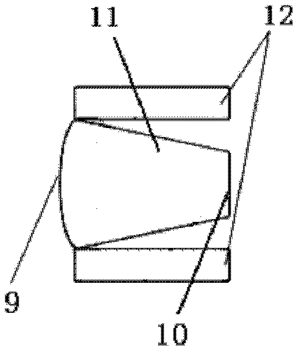
[0011] Depend on figure 2 As shown, the front surface 9 of the non-imaging condenser lens 2 is a spherical surface, the rear surface 10 is a plane, and the side surface 11 is a free-form surface designed according to the princip...


PUM


Abstract

The invention provides a laser optical fiber coupling device containing a non-imaging optical element, belonging to the field of semiconductor illumination. The light source comprises a semiconductor laser tube, a non-imaging condensing lens and an optical fiber; the semiconductor laser tube emits light beams; the light beams are converged on the rear surface of the non-imaging condensing lens after passing through the non-imaging condensing lens; and then the light beams enter the optical fiber to form into a laser optical fiber source. According to the device provided by the invention, as the non-imaging condensing lens is adopted, the light emitted by the laser tube can be converged on the rear surface of the non-imaging condensing lens; meanwhile as the front surface aperture of the non-imaging condensing lens is large, the adjusting tolerance is large relative to the position of the laser tube. When the device is installed and positioned, the mechanical precision dependent on the metal holder can be ensured, and no fine adjustment is required. The adjusting process is simple, and the probability of damage of the laser tube and optical fiber due to caused by touching between the optical fiber and the laser tube during adjustment is reduced, so that the rate of finished product is increased, the adjusting time is reduced and the cost is reduced.

Description

technical field [0001] The invention belongs to the field of semiconductor lighting and relates to a laser fiber coupling device containing non-imaging optical elements. Background technique [0002] With the improvement of the performance of semiconductor lasers, laser lighting technology based on semiconductor lasers is more and more widely used in the field of safety protection monitoring. Due to the mode characteristics of the semiconductor laser's own light emission, its light spot is not uniform, and there are bright and dark stripes. Therefore, semiconductor lasers must be shaped and homogenized before they can be used for night lighting. [0003] At present, the commonly used shaping technology is to directly couple the light from the laser tube into the optical fiber. However, due to the relatively thin core diameter of the optical fiber in this coupling method, the distance between the fiber head and the light emitting surface of the laser tube needs to be adjuste...

Claims


Application Information

Patent Timeline
Patent Type & Authority Applications(China)
IPC IPC(8): G02B6/42
Inventor 刘华王尧韩雪冰卢振武
Owner CHANGCHUN INST OF OPTICS FINE MECHANICS & PHYSICS CHINESE ACAD OF SCI
Why Eureka
Try Eureka