Plasma processing apparatus and protection ring thereof

A processing device and plasma technology, applied in semiconductor/solid-state device manufacturing, discharge tubes, electrical components, etc., can solve problems such as back pollution

Inactive Publication Date: 2012-03-07
SHANGHAI HUAHONG GRACE SEMICON MFG CORP
View PDF6 Cites 3 Cited by
  • Summary
  • Abstract
  • Description
  • Claims
  • Application Information

AI Technical Summary

Problems solved by technology

[0004] The problem to be solved by the present invention is to provide a plasma processing device. When the diameter of the wafer to be processed is greater than the outer diameter of the part of the electrostatic chuck that absorbs the wafer, a protective ring can be provided in the device to effectively improve the plasma processing performance of the wafer. Backside Contamination Issues in Process

Method used


Image

  • Plasma processing apparatus and protection ring thereof
  • Plasma processing apparatus and protection ring thereof
  • Plasma processing apparatus and protection ring thereof

Examples


Embodiment Construction

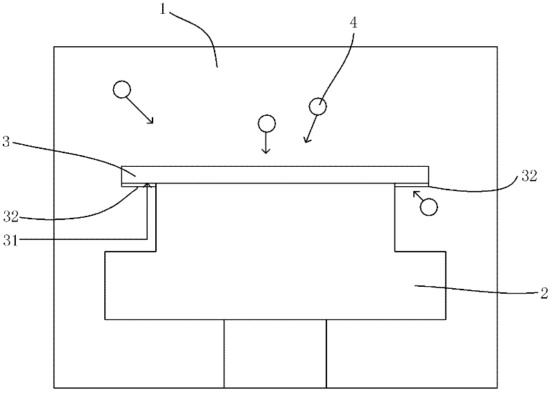
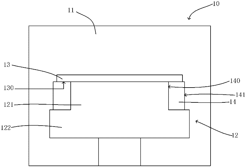
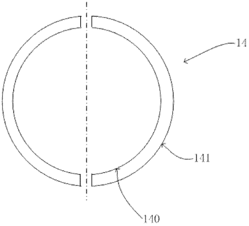
[0020] The problem to be solved by the present invention is: when the diameter of the wafer to be processed is larger than the outer diameter of the portion of the electrostatic chuck that absorbs the wafer, by setting a protective ring in the device, the problem of backside contamination of the wafer during plasma processing can be effectively improved.

[0021] To solve this problem, the present invention sets a hollow annular protective ring in the plasma processing apparatus, which is installed on the electrostatic chuck to surround the electrostatic chuck and supports the wafer to be processed together with the electrostatic chuck. Therefore, the back side of the electrostatic chuck will not be exposed to the plasma in the processing chamber, so that the problem of contamination of the back side of the wafer during the plasma treatment process of the wafer can be improved. Moreover, the size of the guard ring can be flexibly adjusted according to the diameter of the wafer ...


PUM


Abstract

The invention provides a plasma processing apparatus and a protection ring thereof. The plasma processing apparatus comprises the following parts: a processing cavity; a static sucker which is placed in the processing cavity and is applied to adsorb a wafer; a hollow protection ring which is provided on the static sucker in a mode of encircling the static sucker and supports the wafer with the static sucker together. The protection ring is provided on the static sucker and supports a wafer to be processed with the static sucker together. In a process of carrying out plasma processing on the wafer, a wafer back side pollution problem can be improved, and processing strength of the wafer can be increased. A dimension of the protection ring can be flexibly adjusted according to a diameter dimension of the wafer to be processed, and a same plasma processing apparatus can carry out plasma processing on wafers with a plurality of specification dimensions.

Description

technical field [0001] The invention relates to a semiconductor processing device, in particular to a plasma processing device and a protective ring thereof. Background technique [0002] Plasma processing apparatuses widely known in the field of semiconductor manufacturing include chemical vapor deposition (CVD) apparatuses, etching apparatuses, ashing apparatuses, and the like. Such as figure 1 As shown, these plasma processing apparatuses include a processing chamber 1, and an electrostatic chuck 2 is arranged in the processing chamber 1, and a wafer 3, that is, an object to be processed, is arranged on the electrostatic chuck 2. When the wafer 3 needs to be processed, the electrostatic chuck 2 will generate an adsorption force on the wafer 3 and fix the wafer 3 on the electrostatic chuck 2 . [0003] The electrostatic chuck in the plasma processing device is set according to the requirements of the equipment, that is, the electrostatic chuck in the plasma processing de...

Claims


Application Information

Patent Timeline
Patent Type & Authority Applications(China)
IPC IPC(8): H01J37/32H01L21/683
Inventor 周俊杰江瑞星包中诚
Owner SHANGHAI HUAHONG GRACE SEMICON MFG CORP
Why Eureka
Try Eureka