Silicon wafer positioning and loading device applied to chemical mechanical polishing equipment

A loading device and chemical mechanical technology, applied in the field of silicon wafer chemical mechanical polishing equipment and silicon wafer positioning loading device, can solve the problems of vacuum adsorption of silicon wafers, waste of deionized water, increased costs, etc., to achieve automatic loading, improve Efficiency, convenient installation and adjustment

Active Publication Date: 2012-03-14
THE 45TH RES INST OF CETC
View PDF6 Cites 17 Cited by
  • Summary
  • Abstract
  • Description
  • Claims
  • Application Information

AI Technical Summary

Problems solved by technology

[0004] In the current chemical mechanical polishing equipment, the main feature of the silicon wafer loading device is to directly load the silicon wafer by means of vacuum adsorption or water suspension on the carrier. These methods also bring some disadvantages while realizing wafer loading, such as directly controlling the carrier. Vacuum adsorption of silicon wafers is very difficult, and the huge system is likely to break the silicon wafers; when loading silicon wafers with a relatively large diameter, multiple injectors must be used to suspend the silicon wafers in water at the same time. Difficulty with the water pressure of the device, and a lot of deionized water was wasted in the film loading process, which increased the cost

Method used


Image

  • Silicon wafer positioning and loading device applied to chemical mechanical polishing equipment
  • Silicon wafer positioning and loading device applied to chemical mechanical polishing equipment
  • Silicon wafer positioning and loading device applied to chemical mechanical polishing equipment

Examples


Embodiment Construction

[0029] The following will clearly and completely describe the technical solutions in the embodiments of the present invention in conjunction with a preferred embodiment of the present invention and accompanying drawings; obviously, the described embodiments are only some embodiments of the present invention, not all implementations Example: Based on the embodiments of the present invention, all other embodiments obtained by persons of ordinary skill in the art without creative work fall within the protection scope of the present invention.

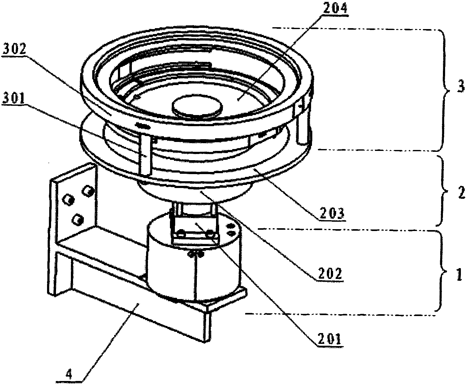
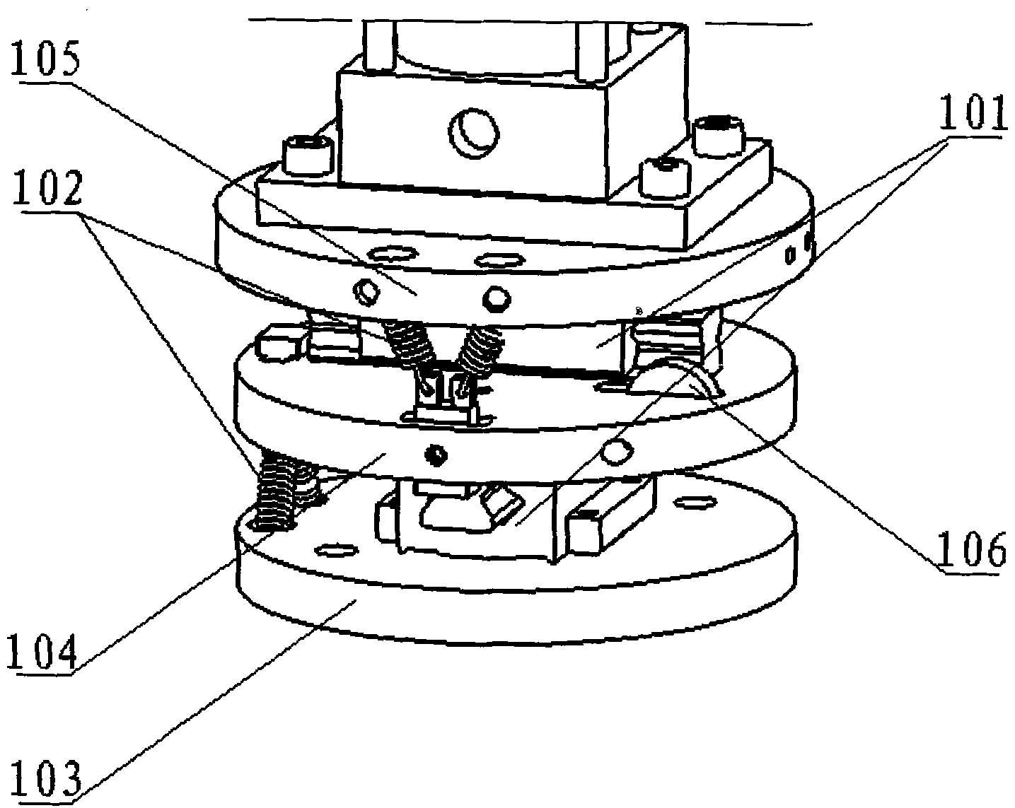
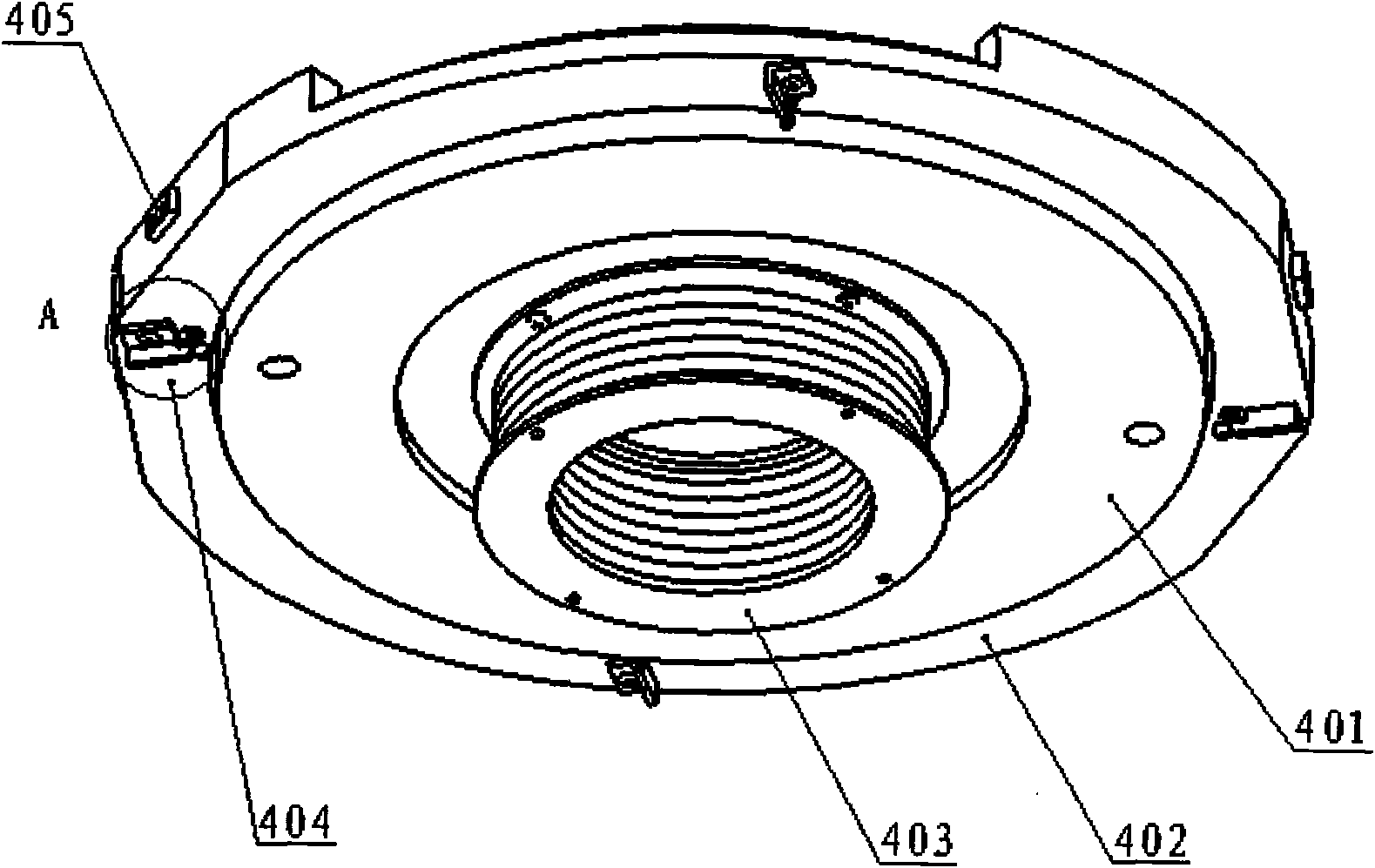
[0030] see Figure 1 to Figure 7, the silicon wafer positioning and loading device used in chemical mechanical polishing equipment has a substrate 203, and the substrate 203 is connected to the upper loading guide ring 302 through a support rod 301; a silicon wafer is placed between the loading guide ring 302 and the substrate 203. space; the fixed part of the lifting drive mechanism 201 is installed on the base plate 203, and the telescop...


PUM


Abstract

The invention provides a silicon wafer positioning and loading device applied to chemical mechanical polishing equipment and relates to the technical field of silicon-wafer chemical mechanical polishing equipment. A base plate of the positioning and loading device is connected to a loading guide ring on the base plate through a supporting rod; a stretching part on a lifting driving mechanism is fixedly connected to a silicon wafer fixture thereon; the silicon wafer fixture is connected to a silicon wafer guide ring outside the silicon wafer fixture; a butt-joint guiding mechanism of a silicon wafer loading device and a silicon wafer resisting-joint guiding mechanism are arranged on the loading guide ring; and an automatic displacement adjusting mechanism and an automatic resetting mechanism are arranged on the base plate or the lower part of the lifting driving mechanism. The positioning and loading device can accurately position a silicon wafer and convey the silicon wafer to a loader for processing. The positioning and loading device has the advantages of simple structure, accurate positioning, loading safety, reliable property and operation convenience, and is beneficial to realizing the automatic loading of the silicon wafer and promoting the efficiencies for positioning, loading and processing the silicon wafer. The positioning and loading device is especially suitable for the loading of the silicon wafer in the chemical mechanical polishing equipment and also can be used for loading wafers during production processes of a transistor and an integrated circuit.

Description

technical field [0001] The invention relates to the technical field of silicon wafer chemical mechanical polishing (CMP) equipment and a silicon wafer positioning and loading device. Background technique [0002] In the production of integrated circuits, most of the processes involve wafer positioning and loading. The effect of wafer positioning and loading has an important impact on wafer processing. Improper handling may cause wafers to be scrapped or manufactured. The performance of the device is poor, and the stability and reliability are poor. Therefore, the development of a high positioning accuracy and efficient wafer positioning and loading method is of great significance for both wafer processing and semiconductor device production. It is precisely because wafer positioning and loading is the most important and frequent step in the manufacture of semiconductor devices, and its efficiency will directly affect the yield, performance and reliability of the device, so ...

Claims


Application Information

Patent Timeline
Patent Type & Authority Applications(China)
IPC IPC(8): B24B37/27
CPCH01L21/68742B24B37/345H01L21/68721H01L21/68785
Inventor 高文泉陈波王伟李久芳
Owner THE 45TH RES INST OF CETC
Why Eureka
Try Eureka