Random storage

A random access memory and storage unit technology, applied in the field of storage processing, can solve problems such as shortening refresh time, increasing leakage, complex logic circuits, etc., and achieve the effect of reducing complexity and improving integration

Active Publication Date: 2013-09-18
GALAXYCORE SHANGHAI
View PDF4 Cites 0 Cited by
  • Summary
  • Abstract
  • Description
  • Claims
  • Application Information

AI Technical Summary

Problems solved by technology

The capacitor C1 of DRAM is generally formed in a stacked or trenched manner. The advantage is that it occupies a small area and can achieve a large capacity. The disadvantage is that the process is much more complicated than the logic circuit, and the access speed is slower than that of SRAM.
Another disadvantage of DRAM is that memory cells are based on the amount of charge stored on capacitor C1, which decreases with time and temperature and must therefore be refreshed periodically to maintain the correct information they originally remembered
Another disadvantage of DRAM is that due to the conductive interconnection between capacitor C1 and MOS transistor M1, there is a contact hole for conductive interconnection, which needs to be in contact with the silicon surface when interconnecting with the MOS transistor. In this way, there will be an interface state at the contact interface between the contact hole and the silicon, and the electrons in the interface state are relatively active (plasma etching is required when making the contact hole, which will cause damage to the chip surface, and the contact of the two interfaces will be damaged at the same time. There are interface states. Due to the existence of interface states, there are a large number of defect centers on the surface, which makes it easy for carriers to be captured and released on the surface, which greatly increases leakage), and leakage is a problem that is very difficult to control, (increased leakage will lead to refresh Time is shortened, power consumption is increased), and DRAM and SRAM will have reset noise when reading and writing
[0005] From the above analysis of the existing technology, it can be seen that the performance of the existing SRAM and DRAM has defects

Method used


Image

  • Random storage
  • Random storage
  • Random storage

Examples


Embodiment Construction

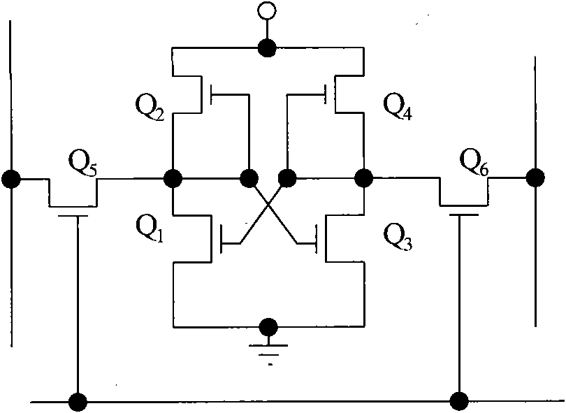
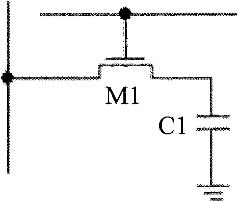
[0042]In view of the above problems, the inventor found through research that, on the one hand, both DRAM and SRAM have reset noise when reading and writing. On the other hand, the existing SRAM occupies a large area, while the DRAM process is much more complicated, and the access speed is slow, and the amount of stored charge decreases with time and temperature, so it must be refreshed regularly. Conductive interconnection between C1 and MOS transistor M1, so there is a contact hole for conductive interconnection, the contact hole needs to be in contact with the silicon surface when interconnecting with the MOS transistor, so that the contact hole and silicon There will be an interface state at the contact interface, and the electrons in the interface state are relatively active (plasma etching is required when making a contact hole, which will cause damage to the chip surface, and at the same time, there will be an interface state in the contact of the two interfaces, due to ...


PUM


Abstract

The invention provides a random storage. The random storage comprises a pre-storing unit, a storing unit, a read-write unit and an output unit, wherein the pre-storing unit is used for storing reference data; the storing unit is used for storing data; the read-write unit is used for writing the data into the storing unit, writing the reference data into the pre-storing unit, reading the reference data stored in the pre-storing unit and the data stored in the storing unit, and generating intermediate data which are related to the data stored in the storing unit and the reference data stored in the pre-storing unit; and the output unit is used for comparing the intermediate data generated by the read-write unit with the reference data and outputting the stored data according to the size relation between the intermediate data and the reference data. Therefore, the performance of the random storage can be improved.

Description

technical field [0001] The invention relates to the field of storage processing, in particular to a random access memory. Background technique [0002] Data stored in a random access memory (RAM, random access memory) can be read or written on demand, and the speed of reading and writing has nothing to do with the storage location of the data. This kind of memory has the fastest read and write speed in the memory, but the stored data will be lost when the power is turned off, so it is mainly used to store short-term data. According to different stored information, random access memory can be divided into static random access memory (Static RAM, SRAM) and dynamic random access memory (Dynamic RAM, DRAM). [0003] An existing SRAM such as figure 1 As shown, its storage unit is a flip-flop, which is composed of 6 MOS transistors, that is, the first MOS transistor Q1, the second MOS transistor Q2, the third MOS transistor Q3, the fourth MOS transistor Q4, the fifth MOS transis...

Claims


Application Information

Patent Timeline
Patent Type & Authority Patents(China)
IPC IPC(8): G11C11/4193
Inventor 赵立新李文强霍介光李杰
Owner GALAXYCORE SHANGHAI
Why Eureka
Try Eureka