cmos active pixel structure and image sensor

A pixel structure and pixel unit technology, applied in the field of image sensing, can solve the problems of reduced sensitivity, complex structure, and reduced pixel filling factor, and achieve the effect of reducing the influence of noise and improving the signal-to-noise ratio

Active Publication Date: 2017-12-29
SHENZHEN UNIV
View PDF9 Cites 0 Cited by
  • Summary
  • Abstract
  • Description
  • Claims
  • Application Information

AI Technical Summary

Problems solved by technology

However, due to the complex circuit structure of the pixel unit, the area of ​​a single pixel is large, which is not conducive to integration; at the same time, the transistor integrated on the surface of the active pixel reduces the area of ​​the photosensitive part of the pixel, which will reduce the pixel fill factor and reduce the sensitivity.

Method used


Image

  • cmos active pixel structure and image sensor
  • cmos active pixel structure and image sensor
  • cmos active pixel structure and image sensor

Examples


Embodiment Construction

[0028] In order to have a clearer understanding of the technical features, purposes and effects of the present invention, the specific implementation manners of the present invention will now be described in detail with reference to the accompanying drawings.

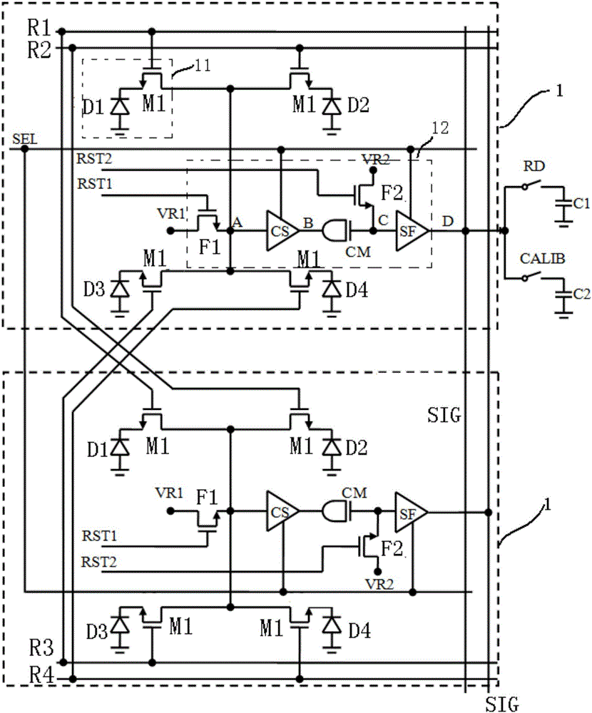
[0029] Such as figure 1 A CMOS active pixel structure 1 in a preferred embodiment of the present invention is shown for use in an image sensor. The CMOS active pixel structure 1 includes a plurality of pixel units 11 and a readout circuit 12 . In this embodiment, there are four pixel units 11 , but it is not limited thereto. The fill factor of the CMOS active pixel structure 1 can be improved by sharing one readout circuit 12 with multiple pixel units 11 .

[0030] The pixel unit 11 includes a photodiode D1 and a transmission tube M1. The readout circuit 12 includes a first reset transistor F1, a second reset transistor F2, an amplifier circuit CS, a MOS capacitor CM, and a source follower SF. Wherein, the output en...


PUM


Abstract

The invention discloses a CMOS active pixel structure and an image sensor. The CMOS active pixel structure includes a plurality of pixel units and a readout circuit for reading out an electrical signal generated by each pixel unit sensing light; The readout circuit includes a first reset transistor, a second reset transistor, an amplifying circuit, a MOS capacitor and a source follower, the output end of each pixel unit is electrically connected to the input end of the amplifying circuit respectively, and the output end of the amplifying circuit , MOS capacitors, and the source follower are electrically connected in sequence, the output end of the first reset transistor is electrically connected to the common node between the output end of each pixel unit and the input end of the amplifying circuit, and the output end of the second reset transistor is The output terminal is electrically connected to the common node of the MOS capacitor and the source follower, and the control terminals of the first reset transistor and the second reset transistor are respectively used for inputting a conduction signal to control the two The voltage at the common node is reset. The invention has the beneficial effects of high signal-to-noise ratio and high filling factor.

Description

technical field [0001] The invention relates to the field of image sensing, in particular to a CMOS active pixel structure and a graphic sensor. Background technique [0002] Widely used image sensors are generally classified into two types: complementary metal oxide semiconductor (CMOS) image sensors and charge coupled device (CCD) image sensors. With the improvement of integrated circuit process technology and design level, CMOS image sensor is widely used in many fields such as digital camera, video camera, printer, scanner due to its high integration, fast readout speed, low power consumption and low cost. , human-machine interface, monitoring and monitoring, machine vision, biological testing, etc., are increasingly challenging CCD image sensors. [0003] A CMOS image sensor generally includes a photoelectric conversion element array, a pixel readout circuit, a column readout circuit, a timing control circuit, and a row and column control circuit. The pixel structure ...

Claims


Application Information

Patent Timeline
Patent Type & Authority Patents(China)
IPC IPC(8): H04N5/374H04N5/3745
Inventor 李琰俞航刘少华姜来纪震
Owner SHENZHEN UNIV
Why Eureka
Try Eureka