A high-speed global exposure pixel structure for intra-pixel correlated double sampling
A related double sampling and pixel structure technology, applied in the field of image sensors, can solve problems such as increased time consumption, decreased imaging frame rate, and inability to achieve double sampling.
- Summary
- Abstract
- Description
- Claims
- Application Information
AI Technical Summary
Problems solved by technology
Method used
Image
Examples
Embodiment Construction
[0019] Below in conjunction with the accompanying drawings in the present invention, the technical solutions in the present invention are further described clearly and completely:
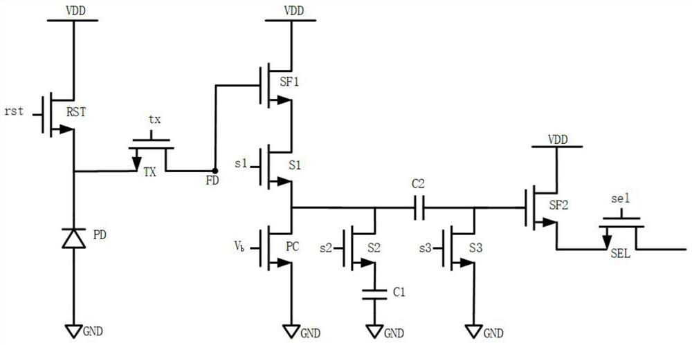
[0020] like figure 1 shown, figure 1 A schematic diagram of a high-speed global exposure pixel structure for realizing intra-pixel correlated double sampling provided by the present invention includes a photodiode (PD), a reset transistor (RST), a charge transfer transistor (TX), two source followers (SF1, SF2), multi-function transistor (PC), three MOS switches (S1, S2, S3), selection transistor (SEL), two capacitors (C1, C2);
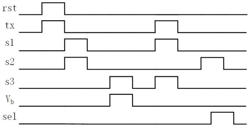
[0021] Among them, the photodiode PD is used to collect the optical signal and convert it into an electrical signal. The signal is read out to the charge-voltage conversion node (FD) through the charge transfer transistor TX. The cathode of the photodiode PD is connected to the reset transistor RST source and charge transfer. The drain of the transistor TX is connected, ...
PUM
 Abstract
Description
Claims
Application Information


