Film forming apparatus and film forming method

A film-forming device and a film-forming method technology, applied in the direction of gaseous chemical plating, coating, electrical components, etc., can solve the problems of film quality decline, falling, and adhesion to the substrate surface, etc., and achieve the effect of simplifying the structure of the device

Inactive Publication Date: 2012-03-14
TOKYO ELECTRON LTD
View PDF3 Cites 5 Cited by
  • Summary
  • Abstract
  • Description
  • Claims
  • Application Information

AI Technical Summary

Problems solved by technology

[0003] However, in the above two methods, in the former method, there is a cold spot (Cold Spot) in the transfer pipe from the container that feeds the raw material to the chamber, or the partial pressure rises, and the temporarily vaporized raw material solidifies on the way. However, it is trapped (trap), so sometimes there is a failure that cannot be delivered to the chamber
In addition, the latter method has the problem that the raw material gas cannot be supplied to the chamber due to the ...

Method used


Image

  • Film forming apparatus and film forming method
  • Film forming apparatus and film forming method
  • Film forming apparatus and film forming method

Examples


no. 1 approach

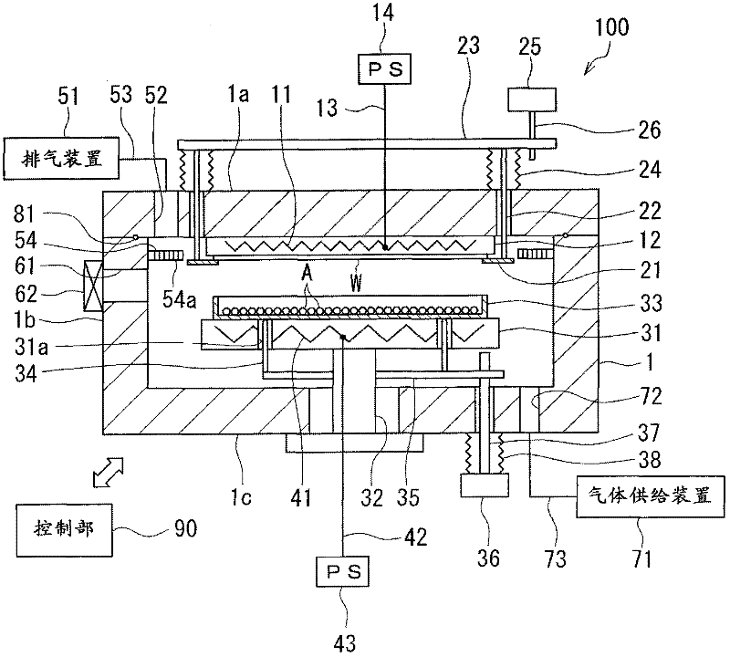
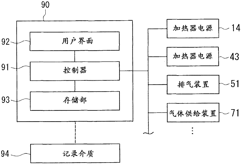
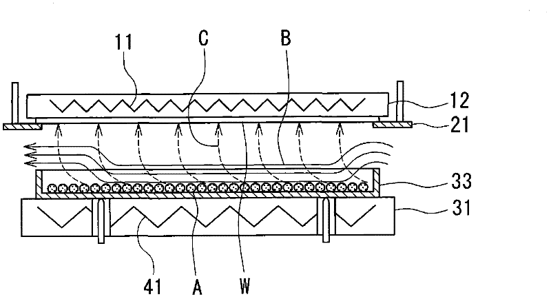
[0030] The film formation apparatus 100 according to the first embodiment of the present invention will be described. First, refer to figure 1 as well as figure 2 , the structure of the film forming apparatus 100 will be described. figure 1 It is a sectional view showing a schematic structure of the film forming apparatus 100 according to the first embodiment, figure 2It is a diagram showing a configuration example of its control system. This film forming apparatus 100 includes, as main configurations, a processing container 1 for accommodating a semiconductor wafer (hereinafter referred to as "wafer W") as a substrate to be processed; a substrate heater 11 as a first heater; and a holding member 21 for holding the wafer W. ; the table 31 as a raw material supporting part; and the raw material heater 41 as a second heater. The film forming apparatus 100 further includes: an exhaust device 51 as an exhaust unit for maintaining the inside of the processing chamber 1 in a v...

no. 2 approach

[0084] Next, a second embodiment of the present invention will be described. Figure 9 It is a cross-sectional view showing a schematic configuration of the film forming apparatus 101 according to the second embodiment. In this embodiment, as means for heating the solid raw material A, a lamp heater is used. In addition, in the following description, the Figure 9 The characteristic structure of the film forming apparatus 101 will be described as the center. For the film forming apparatus 101 and figure 1 The same structures of the film forming apparatus 100 are denoted by the same symbols and descriptions thereof are omitted.

[0085] In the film forming apparatus 101 of the present embodiment, as a raw material support unit, for example, an annular movable member 121 that can be raised and lowered is provided, and the movable member 121 stands upright from the movable member 121 and comes into contact with the bottom surface of the raw material tray 33 to support the raw m...

no. 3 approach

[0094] Next, a third embodiment of the present invention will be described. Figure 11 It is a cross-sectional view showing a schematic configuration of the film formation apparatus 102 according to the third embodiment. In addition, in the following description, the Figure 11 The characteristic structure of the film forming device 102 will be described as the center. For the film forming device 102 and figure 1The same structures of the film forming apparatus 100 are denoted by the same symbols and descriptions thereof are omitted. In the film forming apparatus 102 of this embodiment, the wafer W is held by an electrostatic adsorption mechanism. An electrostatic chuck 151 serving as a substrate holder is embedded in the heat transfer plate 12 disposed in the upper portion of the processing chamber 1 . The electrostatic chuck 151 has a structure in which an unillustrated electrode layer is sandwiched between dielectric layers, and the electrode layer is connected to a DC p...


PUM


Abstract

The invention provides a film forming apparatus and a film forming method. Under the situation of using a solid raw material to form a film, a filming forming raw material gas can be supplied to the surface of a substrate stably and effectively, and the particulate pollution and the possibility that impurities are mixed in the film can be reduced. A film forming apparatus(100) comprises a processing container(1) for accommodating a wafer(W), a substrate heater(11) for heating the wafer(W), a keeping part(21) for keeping the wafer(W), a workbench(31) used as a raw material supporting table and a raw material heater(41) for heating the solid raw material. In the film forming apparatus, for example, on the workbench(31), the solid raw material is heated on one hand, and is reacted with other gasification promoting gas on the other hand, and the generated film forming raw material gas is supplied to the lower surface(a processed surface) of the wafer(W) kept on the keeping part(21), so that the film forming raw material gas generates a thermal decomposition on the surface of the wafer(W) to form the film.

Description

technical field [0001] The present invention relates to a film-forming apparatus and a film-forming method for performing film-forming processing on a semiconductor substrate or the like. Background technique [0002] Conventionally, there has been proposed a film-forming method using a solid raw material when forming a metal film or the like on a substrate as an object to be processed (for example, Patent Document 1). In a film forming apparatus, when a solid raw material having a low vapor pressure is vaporized and the raw material is transported to a chamber, the following method is generally employed. For example, a method is known in which solid raw material powder is put into a container different from the chamber, the solid raw material is heated, and the solid raw material is vaporized while being transported into the chamber by a carrier gas, and the solid raw material is transported to the chamber from above. The film formation object surface of the substrate is s...

Claims


Application Information

Patent Timeline
IPC IPC(8): H01L21/20C23C16/455
CPCC23C16/4488C23C16/45563C23C16/4586
Inventor 军司勋男
Owner TOKYO ELECTRON LTD
Why Eureka
Try Eureka