

Generation method and device of qualified crystal grain distribution pattern
A distribution map and grain technology, applied in the direction of measuring devices, instruments, semiconductor/solid-state device testing/measurement, etc., can solve problems such as errors, inaccurate qualified grain distribution maps, and affecting wafer shipment efficiency, etc., to achieve reduction The effect of manual operation, improving efficiency and accuracy
- Summary
- Abstract
- Description
- Claims
- Application Information
AI Technical Summary
Problems solved by technology
Method used
Image


Examples
Embodiment Construction
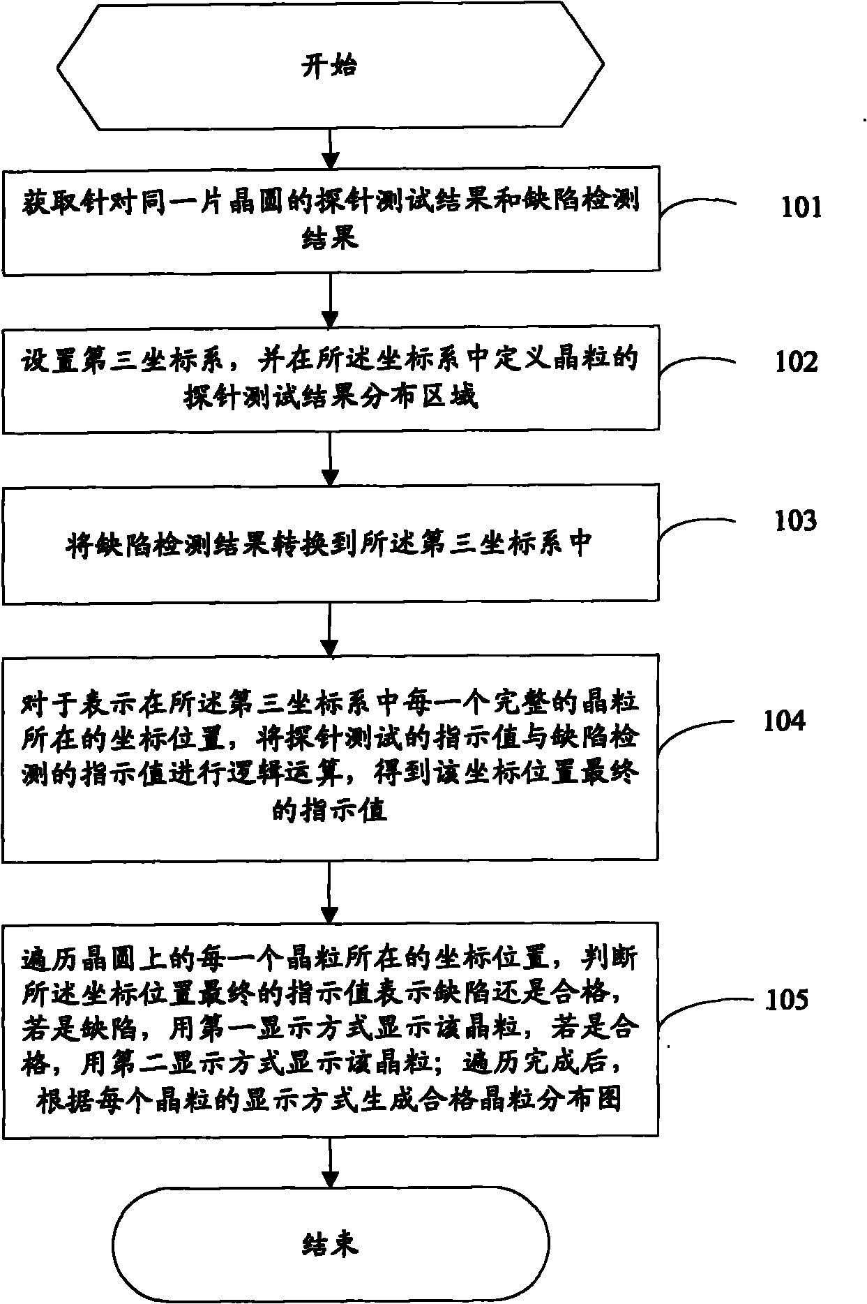
[0037] figure 1 Shown is the generation process of the qualified grain distribution diagram proposed by the embodiment of the present invention, including the following steps:
[0038] Step 101: Obtain probe test results and defect detection results for the same wafer.
[0039] The probe test results include N1 sets of data, and N1 is the total number of dies on the wafer subjected to probe test. Each set of data includes an x coordinate value and a y coordinate value, which are used to indicate the position of the crystal grain corresponding to the set of data on the wafer; the data also includes an indicator value (flag), which is used to indicate the corresponding Whether the die is qualified, for example, a logic 1 is used to indicate that it is not qualified, and a logic 0 is used to indicate that it is qualified. The defect detection result includes N2 sets of data, and N2 is the total number of crystal grains for which defect detection is performed on the wafer. Ea...
PUM
 Abstract
Description
Claims
Application Information