Array substrate, fabrication method thereof and liquid crystal display panel

A technology of an array substrate and a manufacturing method, which is applied in the field of liquid crystal display panels, can solve the problems such as the limitation of the size of the display area 320 and cannot be further enlarged, and achieve the effects of saving the area of ​​scanning line connecting lines, improving display quality, and improving utilization rate.

Active Publication Date: 2012-03-21
SHANGHAI TIANMA MICRO ELECTRONICS CO LTD
View PDF5 Cites 54 Cited by
  • Summary
  • Abstract
  • Description
  • Claims
  • Application Information

AI Technical Summary

Problems solved by technology

This causes the size of the display area 320 to be limited and cannot be further enlarged

Method used


Image

  • Array substrate, fabrication method thereof and liquid crystal display panel
  • Array substrate, fabrication method thereof and liquid crystal display panel
  • Array substrate, fabrication method thereof and liquid crystal display panel

Examples


Embodiment Construction

[0046] In order to solve the above problems, the inventors of the present invention propose a liquid crystal display panel, which includes an array substrate, a color filter substrate, and a liquid crystal layer located between the array substrate and the color filter substrate. The structures of the color filter substrate and the liquid crystal layer are the same as those of the prior art, and the array substrate includes:

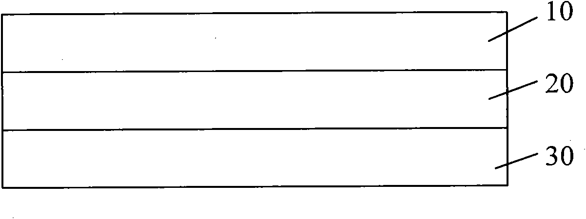
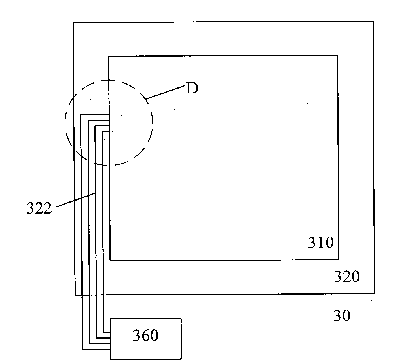
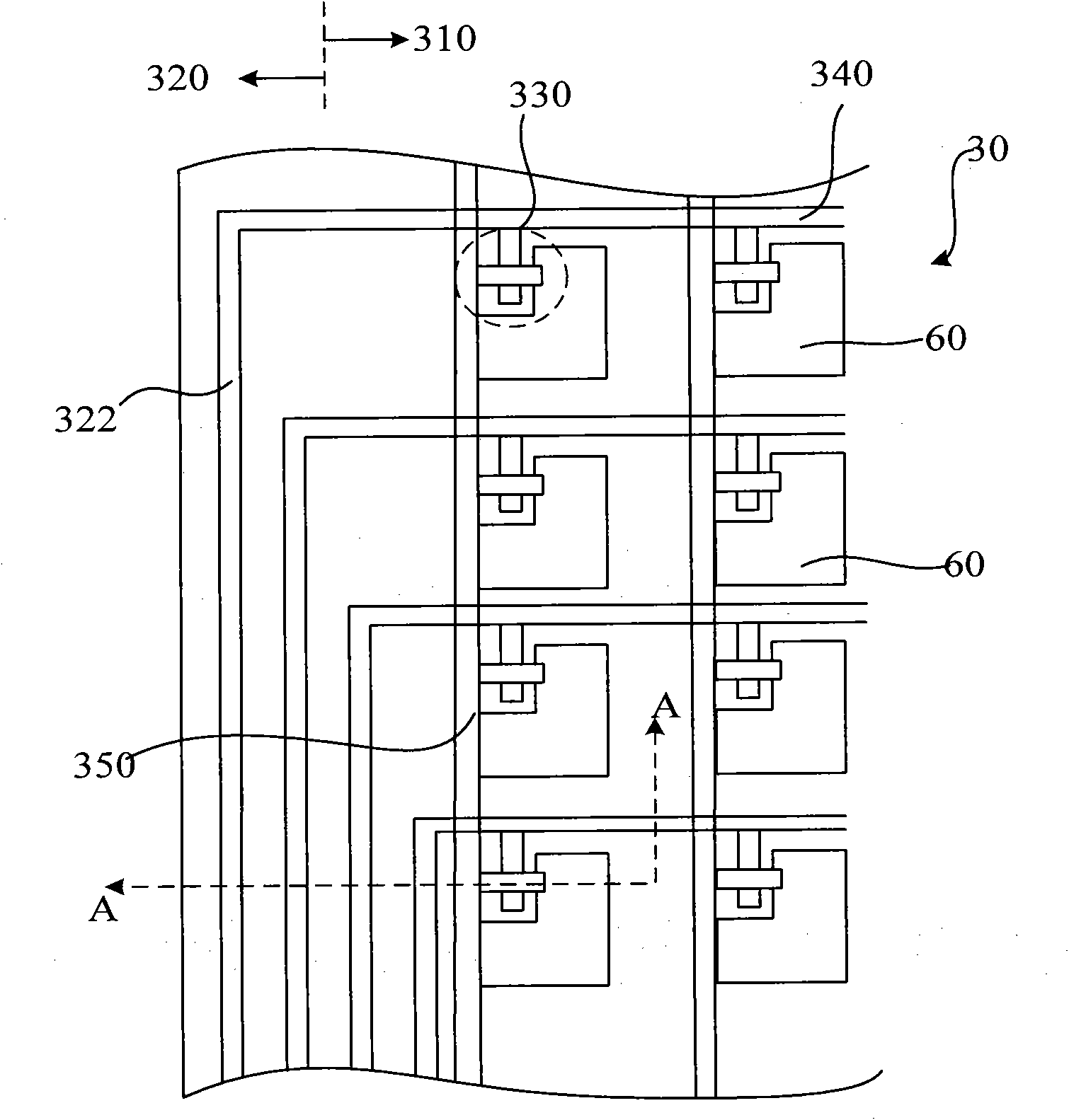
[0047] a substrate, the substrate is divided into a display area and a frame area, and the frame area surrounds the display area;

[0048] a plurality of pixel electrodes arranged in a matrix in the display area;

[0049] A plurality of scanning lines, located between a plurality of pixel electrodes;

[0050] A plurality of data lines are located between the plurality of pixel electrodes, and the data lines intersect with the scanning lines insulated;

[0051]The scanning line connection line is located in the display area, the scanning line connection ...


PUM


Abstract

The invention provides an array substrate, a fabrication method thereof and a liquid crystal display panel comprising the array substrate. The array substrate comprises a substrate, a plurality of pixel electrodes, a plurality of scanning lines, a plurality of data lines and scanning line connection lines; the substrate is divided into a display area and a frame area, and the display area is surrounded by the frame area; the pixel electrodes are arranged in the form of an array in the display area; the scanning lines are positioned among the pixel electrodes; the data lines are positioned among the pixel electrodes, and are insulatively intersected with the scanning lines; and the scanning line connection lines are positioned in the display area, are in parallel with the data lines, and are correspondingly and electrically connected with the scanning lines to transmit the signals of a scanning drive circuit to the corresponding scanning lines. The area of the frame area of the array substrate and the liquid crystal display panel is reduced, consequently, the frame of a liquid crystal display is narrowed, and the utilization rate of the substrate is increased.

Description

technical field [0001] The invention relates to a liquid crystal display panel, in particular to an array substrate for reducing the frame width of the liquid crystal display panel to achieve a narrow frame design, a manufacturing method thereof, and a liquid crystal display panel. Background technique [0002] Flat-panel displays are currently the most popular displays, among which liquid crystal displays are widely used in electronic products such as computer screens, mobile phones, personal digital assistants, and flat-screen TVs because of their thin and light appearance, power saving, and no radiation. [0003] Please refer to figure 1 , for an existing liquid crystal display panel. It includes a color filter substrate 10 and an array substrate 30 opposite to the color filter substrate 10 , and the liquid crystal layer 20 is sandwiched between the color filter substrate 10 and the array substrate 30 . The inner side of the array substrate 30 relative to the color filt...

Claims


Application Information

Patent Timeline
Patent Type & Authority Applications(China)
IPC IPC(8): H01L21/77G02F1/1362H01L27/02G02F1/1343G02F1/133G02F1/1333
Inventor 李治福刘金娥赵剑
Owner SHANGHAI TIANMA MICRO ELECTRONICS CO LTD
Why Eureka
Try Eureka