Imaging element, drive device for an imaging element, drive method for an imaging element, image processing device, program, and imaging device
A technology of image processing device and camera element, which is applied in the field of programs, camera devices and image processing devices, to achieve the effects of improving sensitivity, reducing power consumption, and increasing frame rate
- Summary
- Abstract
- Description
- Claims
- Application Information
AI Technical Summary
Problems solved by technology
Method used
Image

Examples
no. 1 Embodiment approach
[0050] Next, a first embodiment which is one embodiment of the present invention will be described with reference to the drawings.
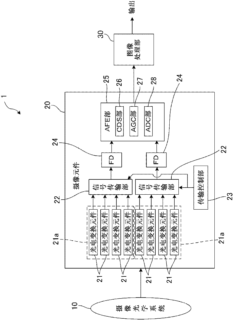
[0051] figure 1 It is a block diagram showing the configuration of the imaging device 1 according to the first embodiment which is one embodiment of the present invention. Such as figure 1 As shown, the imaging device 1 is composed of the following parts: the imaging optical system 10, which guides the subject image to the imaging element 20, and makes it form an image; the imaging element 20, which performs photoelectric conversion on the imaged object image and outputs and an image processing unit 30 that applies predetermined signal processing to the output signal output from the imaging element 20 to reproduce a subject image. Based on the image data corresponding to the image of one frame output from the image processing unit 30, the image data of the still image is generated, and based on the image data corresponding to the plurality of f...
no. 2 Embodiment approach
[0119] Below, refer to Figure 8 A second embodiment which is another embodiment of the present invention different from the first embodiment will be described. The difference between the second embodiment and the first embodiment lies in the specific circuit configuration of the imaging element 20 and its control method, and other configurations are the same as those of the first embodiment, and thus description thereof will be omitted.
[0120] Figure 8 It is a specific circuit configuration diagram of the imaging element of the second embodiment. exist Figure 8 A circuit is shown in which three unit circuits 140 corresponding to the unit grid of the Bayer array are arranged in the row direction and two in the column direction. In the actual circuit configuration, a number equivalent to the total number of pixels of the imaging element of the second embodiment is arranged in the row direction and the column direction, Figure 8 The unit circuit 140 and its surrounding ...
no. 3 Embodiment approach
[0129] Below, refer to Figure 9 A third embodiment which is another embodiment of the present invention will be described. The third embodiment differs from the first embodiment in that the imaging element supports interlace output in which odd-numbered field output for outputting odd-numbered lines and even-numbered field output for outputting even-numbered lines are alternately repeated. In addition, in the third embodiment, the addition mode of the pixel signal in the imaging element is configured differently from that in the first embodiment, thereby allowing the imaging element to support interlaced output.
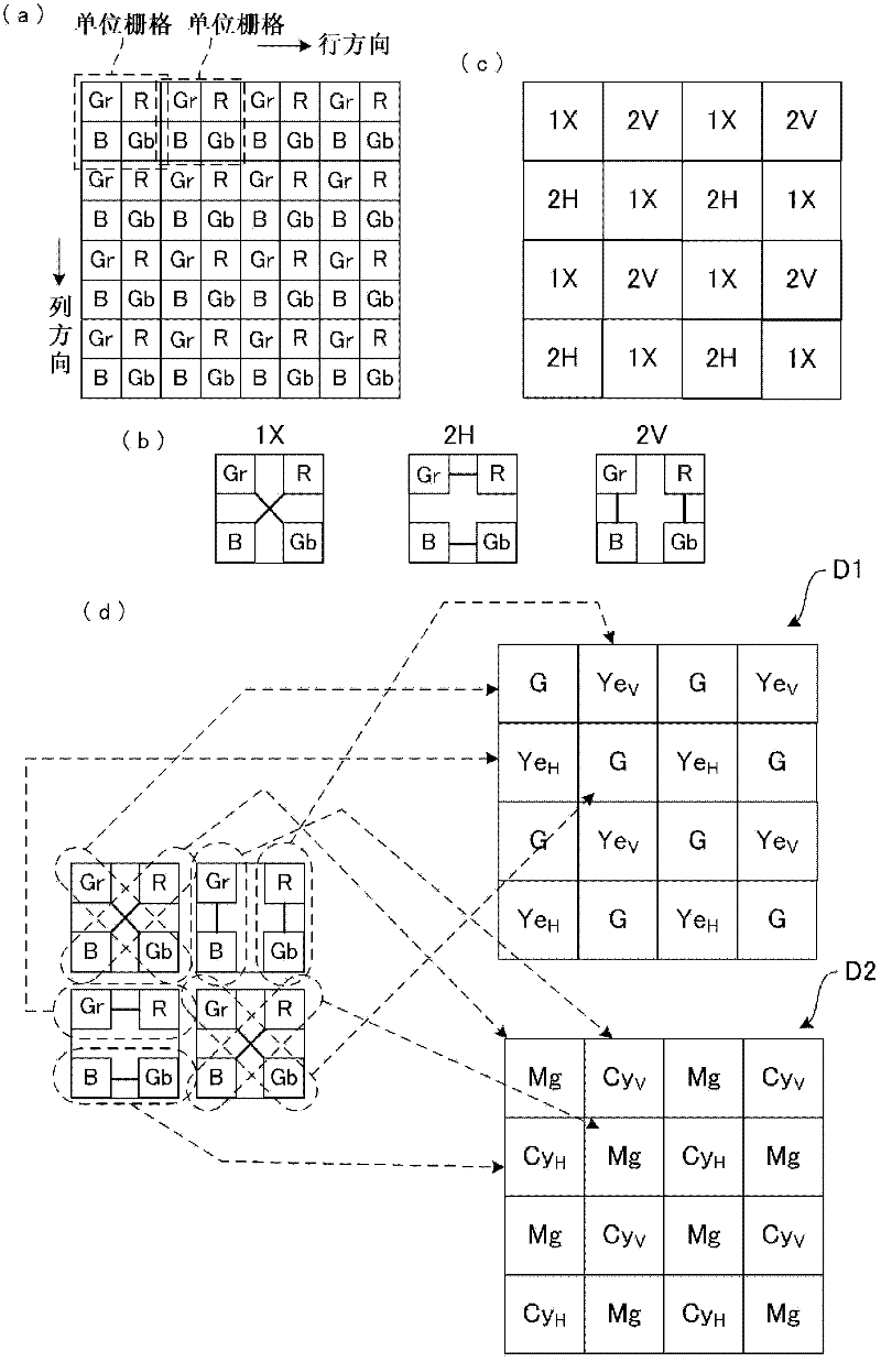
[0130] Figure 9 (a) and Figure 9 (f) represents the substitution adopted in the third embodiment figure 2 In (c), configuration of the addition mode when pixel signals are added. Figure 9 (a) represents the configuration of the addition mode corresponding to the odd field output, Figure 9 (f) shows the configuration of the addition mode corresponding to ev...
PUM
 Abstract
Description
Claims
Application Information
 - R&D
- Intellectual Property
- Life Sciences
- Materials
- Tech Scout
- Unparalleled Data Quality
- Higher Quality Content
- 60% Fewer Hallucinations
Browse by: Latest US Patents, China's latest patents, Technical Efficacy Thesaurus, Application Domain, Technology Topic, Popular Technical Reports.
© 2025 PatSnap. All rights reserved.Legal|Privacy policy|Modern Slavery Act Transparency Statement|Sitemap|About US| Contact US: help@patsnap.com