

Epoxy resin composite material
A technology of epoxy resin and composite materials, which is applied in the chemical field, can solve the problems of adding silicon wafers, etc., and achieve the effects of improving yield, good economic benefits and market prospects, and reducing edge collapse rate
- Summary
- Abstract
- Description
- Claims
- Application Information
AI Technical Summary
Problems solved by technology
Method used
Image

Examples
Embodiment 1
[0020] Example 1 Proportion screening experiment of epoxy resin glue and fused silica powder
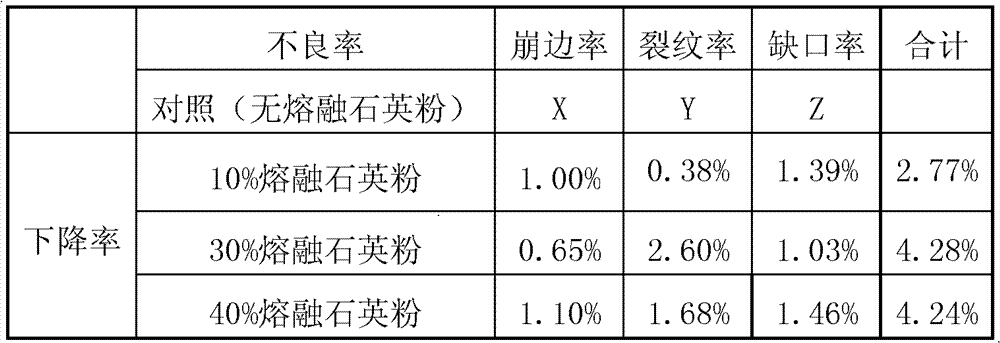
[0021] 1. Experimental materials: Epoxy resin glue is AB two-component glue of Loctite 3382 from Henkel, Germany. Among them, A glue is glycidyl ether epoxy resin glue, B glue is polythiol curing agent, and the added powder The body material is fused silica powder, the expansion coefficient of the fused silica powder is 0.4PPM, and the average particle size D50 is 5 microns.
[0022] Their matching is as shown in Table 1:
[0023] Table 1 Proportion of epoxy resin glue and fused silica powder
[0024] Additive ratio
A glue weight (g)
Fused silica powder weight (g)
B glue weight (g)
10%
22.5
2.5
25
30%
17.5
7.5
25
40%
15
10
25
[0025] 2. Experimental method
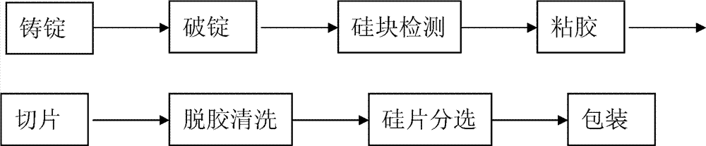
[0026] Silicon wafer manufacturing process such as figure 1 Shown, wherein, viscose process comprises the steps:
[0...
PUM
| Property | Measurement | Unit |
|---|---|---|
| particle size | aaaaa | aaaaa |
| particle size | aaaaa | aaaaa |
| thickness | aaaaa | aaaaa |
Abstract
Description
Claims
Application Information