A kind of cleaning method of diamond wire cut crystalline silicon wafer

A diamond wire cutting and crystalline silicon wafer technology, which is applied in the directions of cleaning methods, cleaning methods and utensils, chemical instruments and methods using liquids, etc., can solve the problem of increasing the fragmentation rate of crystalline silicon wafers, inability to separate crystalline silicon wafers, and difficulty in slicing and other problems, to achieve the effect of reducing the fragmentation rate, reducing the edge collapse rate, and shortening the process time

Active Publication Date: 2019-09-20
CSI CELLS CO LTD +1
View PDF7 Cites 0 Cited by
  • Summary
  • Abstract
  • Description
  • Claims
  • Application Information

AI Technical Summary

Problems solved by technology

[0005] However, when cutting silicon wafers, especially crystalline silicon wafers, with a diamond wire saw, there are many fragments and high loss during the pre-cleaning of the inserted wafers, and it is difficult to segregate perpendicular to the cutting direction.
[0006] However, the existing cleaning process of inserting a mortar wire saw cannot effectively separate the crystalline silicon wafers, and it is easy to cause an increase in the fragmentation rate of the crystalline silicon wafers

Method used


Image

  • A kind of cleaning method of diamond wire cut crystalline silicon wafer
  • A kind of cleaning method of diamond wire cut crystalline silicon wafer
  • A kind of cleaning method of diamond wire cut crystalline silicon wafer

Examples


Embodiment 1

[0063] Embodiment 1 provides a kind of cleaning method of the crystalline silicon of diamond wire cutting, comprises the steps:

[0064] (1') Slicing the ingot in a fully automatic chip cleaning agent, peeling off the crystalline silicon chip with horizontal force, and inserting the chip to obtain a tooling including the crystalline silicon chip;

[0065] (1) placing the tooling of step (1') including the crystalline silicon wafer in the first washing tank with pure water, to carry out the first pre-cleaning;

[0066] (2a) placing the tooling including the crystalline silicon wafer in step (1) in the second washing tank equipped with an acid cleaning agent, and performing acid cleaning; the acid cleaning adopts citric acid;

[0067] (2b) placing the tooling including the crystalline silicon wafer in step (2a) in the third washing tank equipped with pure water, and washing with water;

[0068] (2c) Place the tooling including the crystalline silicon wafer in step (2b) in the f...

Embodiment 2

[0077] Embodiment 2 provides a kind of cleaning method of the crystalline silicon of diamond wire cut, and the difference with embodiment 1 is: carry out step (3e) between step (3d) and step (4) and step (3d) comprises crystal The tooling of the silicon wafer is placed in the tenth washing tank filled with pure water for the fifth rinse;

[0078] Afterwards, step (4) is carried out, and the workpiece including the crystalline silicon wafer in step (3e) is dried at 65°C.

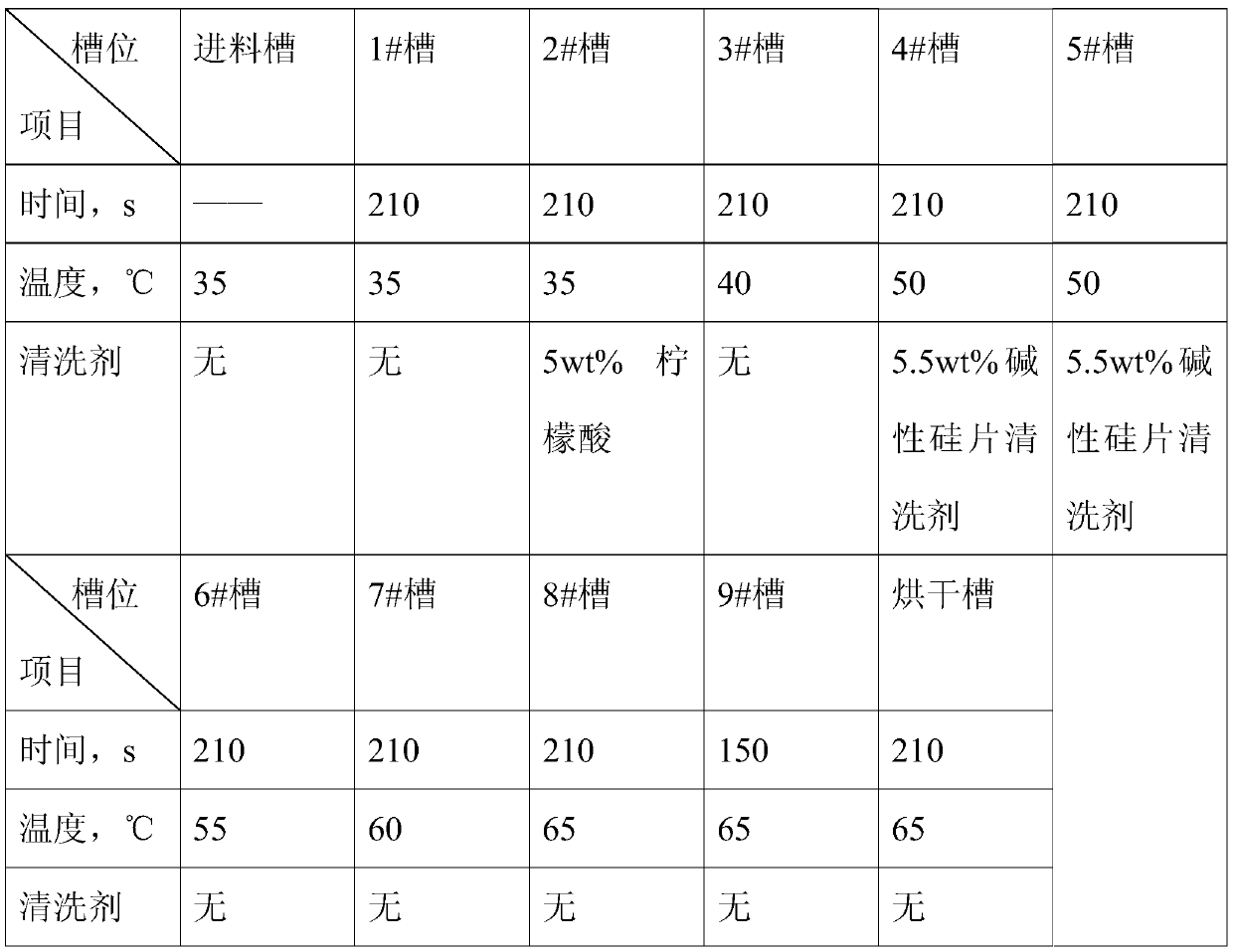
[0079] Adopt the above-mentioned method to carry out the cleaning of crystalline silicon chip, the concrete technological condition of step (1)~(4) is as follows, and the washing quantity is 19000~20000 pieces:

[0080]

Embodiment 3

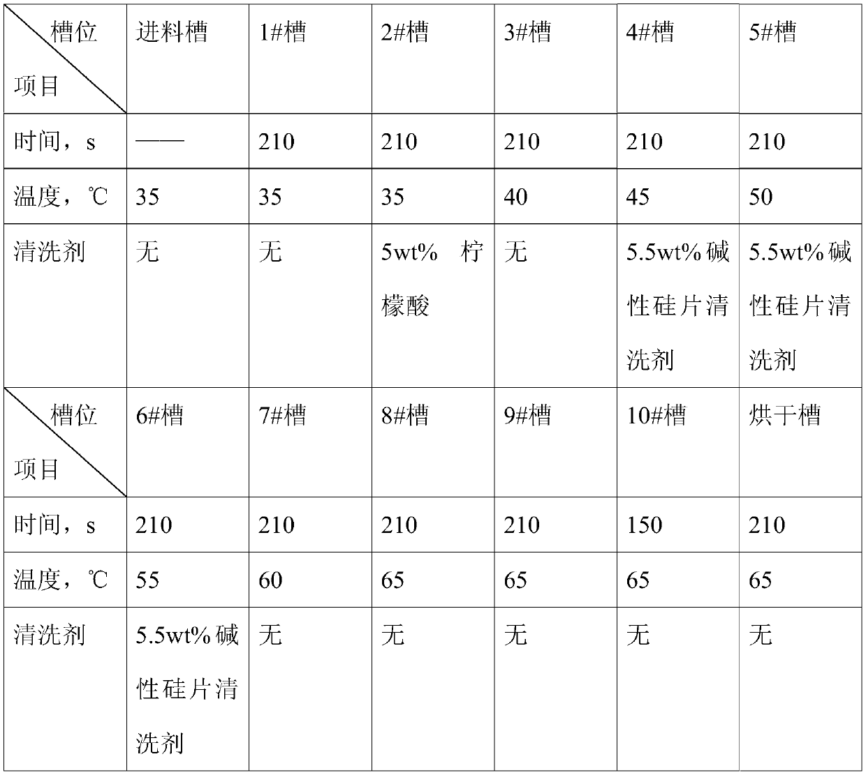
[0082] Provided is a method for cleaning diamond wire-cut crystalline silicon, comprising the steps of:

[0083] (1') Slicing the ingot in a fully automatic chip cleaning agent, peeling off the crystalline silicon chip with horizontal force, and inserting the chip to obtain a tooling including the crystalline silicon chip;

[0084] (1) placing the tooling of step (1') including the crystalline silicon wafer in the first washing tank with pure water, to carry out the first pre-cleaning;

[0085] (2a) Place the tooling including the crystalline silicon wafer in step (1) in the fourth washing tank equipped with a cleaning agent, and perform the first alkali cleaning; the alkali cleaning uses Sanda Oak silicon wafer cleaning agent;

[0086] (3a) placing the tooling including the crystalline silicon wafer in step (2a) in the sixth washing tank equipped with pure water, and rinsing for the first time;

[0087] (3b) placing the tooling including the crystalline silicon wafer in step...


PUM


Abstract

The invention relates to a method of cleaning a crystal silicon wafer cut by a diamond wire saw. The method comprises the following steps: (1)precleaning: (2) cleaning with a reagent; (3) rinsing; and (4) drying; according to the sequence of the working procedure steps, the treatment temperature is gradually raised step by step; the drying temperature in the step (4) is equal to or higher than 65 DEG C; each technological unit comprises a cleaning tank; the temperature of the cleaning tank of a first precleaning technological unit in the step (1) is 30-35 DEG C lower than the drying temperature; the temperature D-value of two adjacent cleaning tanks is equal to or lower than 10 DEG C; and the soaking time of a crystal silicon wafer in each cleaning tank is equal to or shorter than 210 s. According to the invention, proper cleaning technology, cleaning tank temperature and soaking time are selected to obtain the cleaning method suitable for the crystal silicon wafer cut by the diamond wire saw; and with adoption of the method, the crystal silicon wafer can be effectively cleaned, the edge breakage rate, crystal silicon wafer breakage rate and manufacture procedure loss can be reduced, and the technological time also can be shortened.

Description

technical field [0001] The invention belongs to the technical field of crystalline silicon processing, in particular to a method for cleaning crystalline silicon cut by diamond wires. Background technique [0002] Diamond wire sawing is also known as diamond wire sawing or diamond wire sawing. Diamond wire sawing technology has outstanding advantages such as high cutting rate, small environmental load, and low overall cost; it gradually replaces mortar wire sawing technology in the field of solar silicon wafer cutting , become the mainstream technology. [0003] The process of diamond wire cutting is as follows: a silicon ingot square rod is bonded to a substrate through an adhesive to form a workpiece, and then a wire saw fixed with a diamond wire is used to cut the workpiece to obtain a polycrystalline silicon wafer. The workpiece has figure 1 The structure shown has a substrate 100, an adhesive layer 200, and a crystalline silicon wafer 300 bonded to the substrate 100 t...

Claims


Application Information

Patent Timeline
Patent Type & Authority Patents(China)
IPC IPC(8): B08B3/08B08B3/12B08B3/10
Inventor 王珊珊李飞龙邢国强
Owner CSI CELLS CO LTD
Why Eureka
Try Eureka