
Light emitting diode (LED) device and production method thereof

A technology for LED devices and manufacturing methods, applied to semiconductor devices, semiconductor devices of light-emitting elements, reflectors, etc., can solve the problems of small light-emitting angle and uneven light-emitting, and achieve improved light-emitting angle, uniform light-emitting, and uniform light intensity distribution Effect

Inactive Publication Date: 2012-05-02
SICHUAN SUNFOR LIGHT
View PDF0 Cites 25 Cited by
  • Summary
  • Abstract
  • Description
  • Claims
  • Application Information

AI Technical Summary

Problems solved by technology

[0007] In view of this, the present invention provides an LED device and a manufacturing method thereof to solve the problems of small light emitting angle and uneven light emission of existing LED devices

Method used


Image

  • Light emitting diode (LED) device and production method thereof
  • Light emitting diode (LED) device and production method thereof
  • Light emitting diode (LED) device and production method thereof

Examples


Embodiment 1

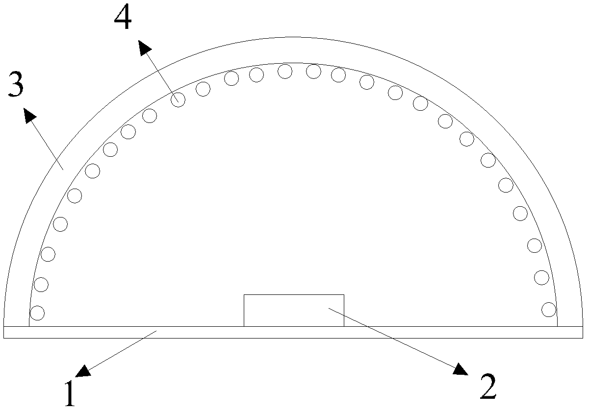
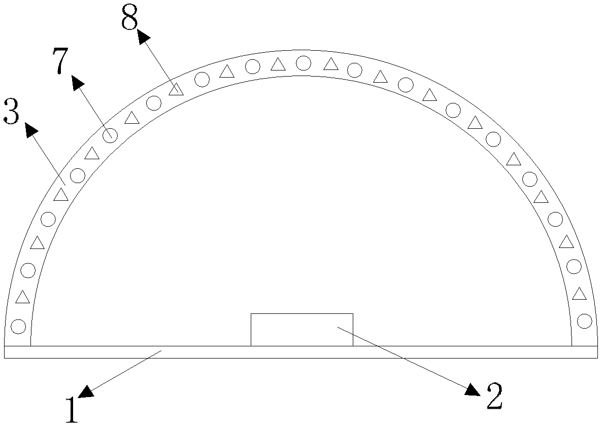
[0042] refer to image 3 , the LED device provided in this embodiment includes: a substrate 1; a chip 2 located on the substrate 1; a lens 3 located on the substrate 1 and covering the chip 2; particle layer. image 3 The shape of middle lens 3 is arc, certainly, also can be the lens of other shapes in other embodiments, for example be the lens of inverted U shape, refer to Figure 4 . The setting of the lens shape is not particularly limited in the present invention, and the following embodiments of this specification are all described by taking a curved lens as an example. In addition, when the lens 3 is a flat lens, it cannot be arranged to cover the chip 2 , and it only needs to be arranged so that the lens 3 and the chip 2 are placed opposite to each other.

[0043] The particle layer can also be coated on the inner surface or the outer surface of the lens, which is not particularly limited in the present invention.

[0044] The particle layer in this embodiment inclu...

Embodiment 2

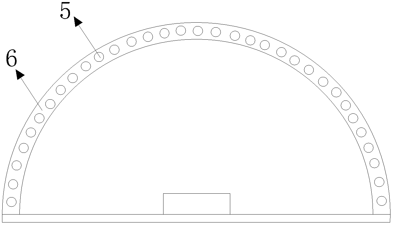
[0049] refer to Figure 5 , The LED device provided in this embodiment includes: a substrate 1; a chip 2 located on the substrate 1; a lens 9 located on the substrate 1 and covering the chip 2; a second lens arranged inside the lens 9 A particle layer.

[0050] The first particle layer can also be coated on the inner surface or the outer surface of the lens 9, which is not particularly limited in the present invention.

[0051] In this embodiment, the first particle layer includes fluorescent powder 7 and reflective particles 10 .

[0052] During the specific working process, the light emitted by the chip 2 is irradiated on the first particle layer, a part of the light is irradiated on the fluorescent powder 7 to excite the phosphor 7 to emit light, and a part of the light is irradiated on the reflective particles 10 to scatter around and to the direction of the substrate 1 Reflection, part of which passes through the phosphor powder 7 and the reflective particles 10 and is ...

Embodiment 3

[0056] refer to Figure 6 , on the basis of Embodiment 1, the LED device provided in this embodiment further includes: a reflective layer 11 disposed on the substrate 1 . When there is a reflective layer 11 in the LED device, the chip 2 and the lens 3 are located on the reflective layer 11 .

[0057] In this embodiment, the purpose of setting the reflective layer 11 on the substrate 1 is: the light emitted by the chip 2 irradiates on the light diffusing particles 8 and will be scattered around, and part of it will be scattered towards the substrate 1. When the reflective layer 11 is set on the substrate 1 Afterwards, the light scattered on the light-reflecting layer 11 will be reflected by the light-reflecting layer 11 so as to shoot to the particle layer, thereby increasing the utilization efficiency of the light emitted by the chip 2. Therefore, the LED device in this embodiment has a large light-emitting angle and light-emitting Uniformity, while further improving the ligh...


PUM

PropertyMeasurementUnit
Beam angleaaaaaaaaaa
Particle sizeaaaaaaaaaa

Abstract

The embodiment of the invention discloses a light emitting diode (LED) device and a production method thereof. The LED device comprises a substrate, a chip, a first lens and a first particle layer, wherein the chip is arranged on the substrate; the first lens is arranged to be opposite to the substrate, and the chip is arranged between the substrate and the first lens; the first particle layer is arranged on the inner surface, on the outer surface or inside the first lens, and the first particle layer comprises fluorescent powder and also comprises light diffusion particles or reflection particles; and the light diffusion particles can scatter the light emitted by the chip and the fluorescent powder, and the reflection particles can reflect the light emitted by the chip. The LED device has high light emitting efficiency, and can solve the problems of the prior art that the LED device has small light emitting angle and non-uniform light.

Description

technical field [0001] The invention relates to the technical field of lighting equipment, and more specifically, to an LED device and a manufacturing method thereof. Background technique [0002] As a new type of solid light source, LED (light-emitting diode) device not only has the advantages of low power consumption, small size, fast response speed, long working life, easy dimming and color adjustment, energy saving and environmental protection, but also has advantages in production, manufacturing and applicability. It also greatly surpasses traditional light sources such as incandescent lamps and fluorescent lamps, so it has made great progress since its birth in the 1960s. At present, it has been widely used in various lighting fields such as street lighting, landscape lighting, large-screen display, traffic signal lights, and indoor lighting. [0003] The mainstream LED device is mainly obtained by exciting yellow phosphor powder with blue light. The traditional proce...

Claims


Application Information

Patent Timeline
IPC IPC(8): H01L33/60H01L33/00
CPCH01L33/00H01L33/60H01L2933/0091F21K9/56H01L33/507F21V3/12F21V3/10F21K9/64F21V7/00F21K9/90
Inventor 王森赵昆
Owner SICHUAN SUNFOR LIGHT
Learn More