Designing method for multi-partition optical phase plate in photo-etching illumination

A design method and phase plate technology, which are applied in the field of microlithography, can solve the problems of large amount of calculation, long time consumption, and inability to meet actual use requirements.

Active Publication Date: 2011-06-29
BEIJING GUOWANG OPTICAL TECH CO LTD
View PDF3 Cites 8 Cited by
  • Summary
  • Abstract
  • Description
  • Claims
  • Application Information

AI Technical Summary

Problems solved by technology

For excimer lasers used in lithography machines, the position, size and light intensity distribution of the beam have obvious jitter and instability; and because there is usually a transmission distance of 5 to 20 meters between the laser and the lighting system of the lithography machine, The relative change between the laser and the lithography machine installation foundation is inevitable. Although technical measures have been taken to stabilize the position and light intensity of the laser beam in the lighting system, this effect has not been completely eliminated.
The current design method can no longer meet the needs of actual use
[0006] 2. The design requires a large amount of computation, takes a long time, and requires high computing equipment
Since the laser wavelengths used in mainstream lithography machines are in the ultraviolet band, such as 193nm and 248nm, etc., the size of the phase unit of the optical phase plate is limited, so when the overall size is determined, the number of units is very large, so the calculation is very large , and need to store a large amount of data

Method used


Image

  • Designing method for multi-partition optical phase plate in photo-etching illumination
  • Designing method for multi-partition optical phase plate in photo-etching illumination
  • Designing method for multi-partition optical phase plate in photo-etching illumination

Examples


Embodiment Construction

[0048] The present invention will be further described below in conjunction with the accompanying drawings and embodiments, but the protection scope of the present invention should not be limited thereto.

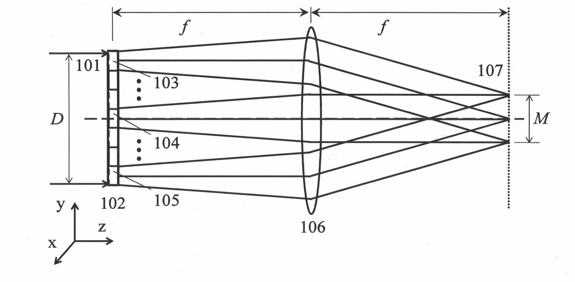
[0049] see first figure 1 , figure 1 It is a schematic diagram of the working principle of the partitioned optical phase plate 102 of the present invention, illustrating an optical path diagram for forming the required light intensity distribution with the thin lens 106 . After the parallel and completely collimated incident light beam 101 passes through each division of the optical phase plate 102, it will form sub-beams with small divergence angles due to diffraction, and these sub-beams will form the desired light on the image plane 107 after passing through the thin lens 106 strong distribution.

[0050] The optical phase plate 102 and the image plane 107 are located on the front focal plane and back focal plane of the thin lens 106 respectively, that is, the distance...


PUM


Abstract

The invention relates to a designing method for a multi-partition optical phase plate in photo-etching illumination, which is characterized by comprising the following steps of: (1) calculating the size l of a phase unit; (2) selecting the partition size d of the optical phase plate; (3) emitting a light beam and determining the light distribution of required light beam, and carrying out matrix process; (4) assigning the initial phase in one partition in the phase plate; (5) processing discretization process with iterative algorithm to obtain the phase distribution of the partition; (6) repeating the step (4) and the step (5) in each partition one by one to obtain the phase distribution of each partition and combine the phase distribution so as to obtain the integral phase distribution; and (7) estimating the designing result. The optical phase plate designed by the invention has the characteristic of insensitivity property for position, size, shape and light distribution of the emitted light beam so that the required output light distribution can be obtained.

Description

technical field [0001] The invention belongs to the field of microlithography, and relates to very large-scale integrated circuit manufacturing equipment, in particular to a design method of a multi-section optical phase plate used for lithography illumination. Background technique [0002] In the illumination system of a lithography machine, in order to improve the quality of lithography, various resolution enhancement technologies are usually used, and off-axis illumination is one of the important technologies. Off-axis illumination technology converts the light intensity distribution in the cross-section of the laser output beam into a specific light intensity distribution that can improve imaging resolution. This specific light intensity distribution can be used for different mask patterns. The distribution can also be a uniform circular distribution. Generally, the light source of the lighting system is usually an excimer laser operating in the form of a pulse. The las...

Claims


Application Information

Patent Timeline
IPC IPC(8): G02B27/00G03F7/20
Inventor 朱菁胡中华杨宝喜陈明曾爱军黄惠杰
Owner BEIJING GUOWANG OPTICAL TECH CO LTD
Why Eureka
Try Eureka