Silicon wafer object table temperature control system of lithography machine and control method thereof

A technology of temperature control system and control system, applied in the direction of temperature control, control/regulation system, non-electric variable control, etc., can solve the problems of equipment utilization rate reduction, process registration accuracy decrease, production capacity decrease, etc., to achieve the best process set The effect of quasi-precision

Active Publication Date: 2012-05-09
SHANGHAI HUALI MICROELECTRONICS CORP
View PDF7 Cites 0 Cited by
  • Summary
  • Abstract
  • Description
  • Claims
  • Application Information

AI Technical Summary

Problems solved by technology

However, in the process of photolithography of silicon wafers using photomasks, when the silicon wafer stage is irradiated by the laser light of the photolithography machine for a certain period of time, heat will occur, and the heat will cause the deformation of the silicon wafer, which will lead to During the continuous operation of the engraving machine, the proc

Method used


Image

  • Silicon wafer object table temperature control system of lithography machine and control method thereof
  • Silicon wafer object table temperature control system of lithography machine and control method thereof
  • Silicon wafer object table temperature control system of lithography machine and control method thereof

Examples


Embodiment Construction

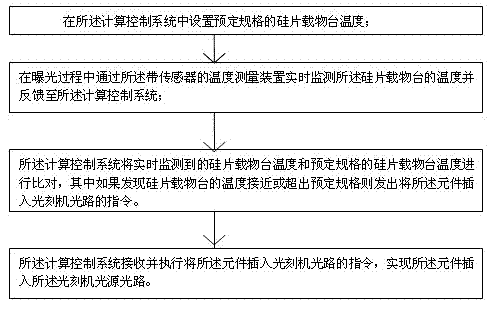
[0017] The present invention will be further described below in combination with principle diagrams and specific operation examples.

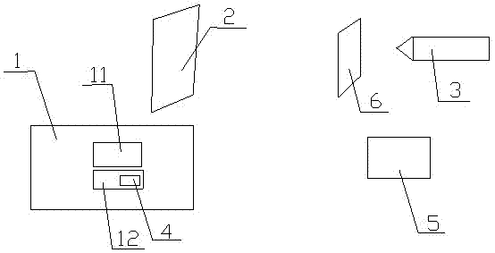
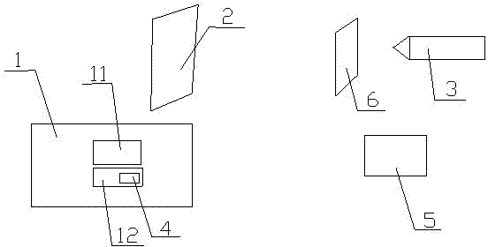
[0018] Such as figure 1 As shown, a silicon wafer stage temperature control system for a photolithography machine of the present invention includes a silicon wafer stage 1, a mask plate 2, and a light source 3 for a photolithography machine, wherein it also includes a temperature measuring device 4 with a temperature sensor, The element 6 and the calculation control system 5, the silicon wafer stage 1 is provided with a silicon wafer placement area 11 and a temperature measurement area 12, the silicon wafer placement area 11 is located at the front end of the temperature measurement area 12, and the temperature measurement area 12 A temperature measuring device 4 with a sensor is provided, the element 6 is located between the light source 3 of the lithography machine and the mask plate 2, the temperature measuring device 4 with a sensor, the ca...


PUM


Abstract

The invention discloses a wafer object table temperature control system of a lithography machine and a control method thereof. The temperature control system comprises a silicon wafer object table, a mask plate and a lithography machine light source, as well as a temperature measurement device with a temperature sensor, an element and a computing control system; a silicon wafer holding area and a temperature measurement area are arranged on the silicon wafer object table; the silicon wafer holding area is located at the front end of the temperature measurement area; the temperature measurement device with the temperature sensor is arranged in the temperature measurement area; the element is located between the lithography machine light source and the mask plate; and the temperature measurement device, the computing control system and the element are connected in series to form a temperature control loop. Through the temperature control system and the control method thereof, the temperature of a silicon wafer during exposure can be controlled, which is beneficial to prevent the deformation of the silicon wafer caused by the temperature, so that better process alignment precision can be obtained and high uniformity among silicon wafers and batches during the continuous service of the lithography machine can be realized.

Description

technical field [0001] The invention relates to a temperature control system and a control method thereof, in particular to a temperature control system and a control method of a silicon wafer stage of a lithography machine. Background technique [0002] The lithography process plays a pivotal role in the current VLSI manufacturing process, and the lithography equipment, process and mask technology are particularly critical to the lithography technology. However, in the process of photolithography of silicon wafers using photomasks, when the silicon wafer stage is irradiated by the laser light of the photolithography machine for a certain period of time, heat will occur, and the heat will cause the deformation of the silicon wafer, which will lead to During the continuous operation of the engraving machine, the process registration accuracy between silicon wafers and batches decreases. In the face of this kind of situation, the industry usually adopts the method of intermit...

Claims


Application Information

Patent Timeline
IPC IPC(8): G03F7/20G05D23/20
Inventor 朱骏
Owner SHANGHAI HUALI MICROELECTRONICS CORP
Why Eureka
Try Eureka