

Wafer surface morphology detection method
A technology of surface topography and topography, applied in the field of detecting wafer surface topography, can solve the problems of complex structure of lithography machine, wafer focusing, increase production cost, etc., and achieve the effect of improving yield, ensuring focusing, and ensuring accuracy
- Summary
- Abstract
- Description
- Claims
- Application Information
AI Technical Summary
Problems solved by technology
Method used
Image

Examples
Embodiment Construction
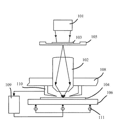
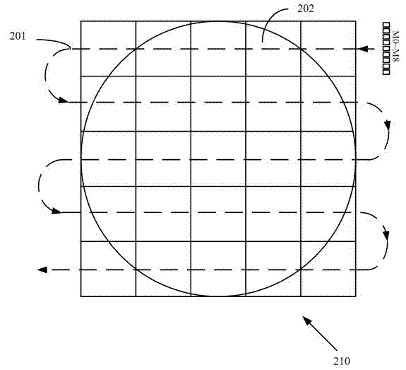
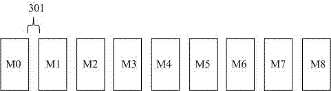
[0028] In the following description, numerous specific details are given in order to provide a more thorough understanding of the present invention. It will be apparent, however, to one skilled in the art that the present invention may be practiced without one or more of these details. In other examples, some technical features known in the art are not described in order to avoid confusion with the present invention.
[0029] In order to thoroughly understand the present invention, detailed steps will be presented in the following description to illustrate how the present invention detects the topography of the wafer surface. Obviously, the practice of the invention is not limited to specific details familiar to those skilled in the semiconductor arts. Preferred embodiments of the present invention are described in detail below, however, the present invention may have other embodiments besides these detailed descriptions.
[0030]In the following paragraphs the invention is ...
PUM
| Property | Measurement | Unit |
|---|---|---|
| Width | aaaaa | aaaaa |
| Width | aaaaa | aaaaa |
| Width | aaaaa | aaaaa |
Abstract
Description
Claims
Application Information