Patterned substrate etching method

A patterned substrate and substrate technology, applied in chemical instruments and methods, crystal growth, electrical components, etc., can solve problems such as high process difficulty and poor graphics, and achieve increased flexibility, smooth side walls, and gentle transitions Effect

Inactive Publication Date: 2012-05-16
BEIJING NAURA MICROELECTRONICS EQUIP CO LTD
View PDF4 Cites 35 Cited by
  • Summary
  • Abstract
  • Description
  • Claims
  • Application Information

AI Technical Summary

Problems solved by technology

[0012] The purpose of the present invention is to at least solve one of the above-mentioned technical defects, especially to solve the defects of poor existing PSS graphics and high process difficulty

Method used


Image

  • Patterned substrate etching method
  • Patterned substrate etching method
  • Patterned substrate etching method

Examples


Embodiment Construction

[0027] Embodiments of the present invention are described in detail below, examples of which are shown in the drawings, wherein the same or similar reference numerals designate the same or similar elements or elements having the same or similar functions throughout. The embodiments described below by referring to the figures are exemplary only for explaining the present invention and should not be construed as limiting the present invention.

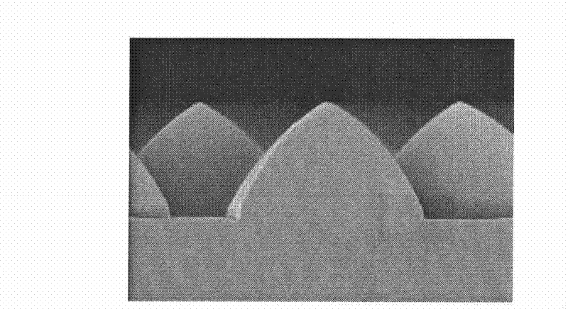
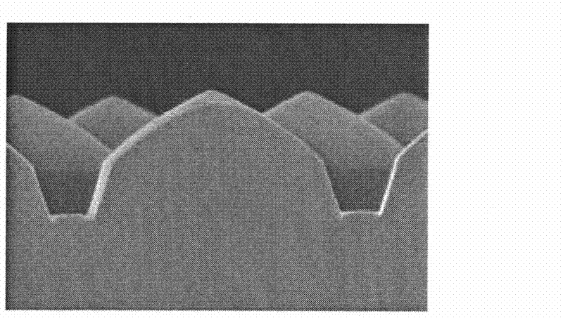
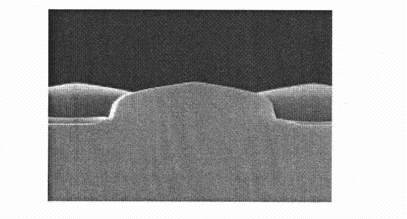
[0028] Such as Figure 4 As shown in FIG. 2 , it is a flow chart of a method for etching a patterned substrate according to an embodiment of the present invention. The method includes the following steps:

[0029] Step S401, providing a substrate. In one embodiment of the present invention, the substrate may be a sapphire substrate. Of course, in other embodiments of the present invention, other substrates may also be used.

[0030] Step S402, forming a photolithography pattern on the substrate.

[0031] In step S403, the substrate ...


PUM


Abstract

The invention provides a patterned substrate etching method. The patterned substrate etching method comprises the following steps of: providing a substrate; forming a photoetched pattern on the substrate; carrying out primary etching on the substrate at a first process pressure and a first bottom radio frequency power by using a first etching gas; and carrying out secondary etching on the substrate at a second process pressure and a second bottom radio frequency power by using a second etching gas, wherein the flow value of the second etching gas is less than that of the first etching gas; the pressure value of the second process pressure is less than that of the first process pressure; and the radio frequency power value of the second bottom radio frequency power is more than that of the first bottom radio frequency power. According to the invention, through twice etching, a PSS (Patterned Substrate) pattern with smooth side wall, smooth transition and no corner can be obtained; the size of the pattern is easy to adjust; and the substrate with good crystal quality is provided for the follow-up film epitaxial process.

Description

technical field [0001] The invention relates to semiconductor technology, in particular to an etching method for a patterned substrate. Background technique [0002] As the world's energy demand continues to rise and natural resources become increasingly scarce, the governments of energy-consuming countries with developed industries are extremely concerned about the development of energy-saving technologies. The continuous progress of GaN-based light-emitting diode (Light Emitting Diode, LED) technology, especially the maturity of blue light-excited phosphor powder to emit yellow light mixed into white light technology, enables daily lighting to achieve low cost and long life. Therefore, governments of various countries have proposed solid-state lighting revolution plans, which have greatly promoted the rapid development of technology and related light-emitting diode technologies. GaN-based LEDs have extremely broad application prospects in image display, signal indication,...

Claims


Application Information

Patent Timeline
Patent Type & Authority Applications(China)
IPC IPC(8): H01L21/02H01L33/00H01L33/20C30B33/12
Inventor 高福宝
Owner BEIJING NAURA MICROELECTRONICS EQUIP CO LTD
Why Eureka
Try Eureka