

Bonding apparatus and bonding method
A bonding device and a technology for bonding parts, which are applied in the manufacture of electrical components, electrical solid devices, semiconductor/solid devices, etc., can solve the problems of large wiring impedance, decreased productivity of wafer bonding processing, and a large amount of time to achieve high-efficiency bonding, The effect of improving productivity
- Summary
- Abstract
- Description
- Claims
- Application Information
AI Technical Summary
Problems solved by technology
Method used
Image

Examples
Embodiment Construction
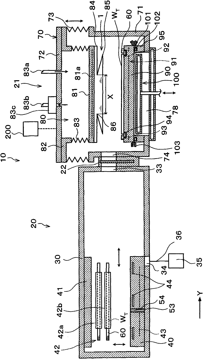
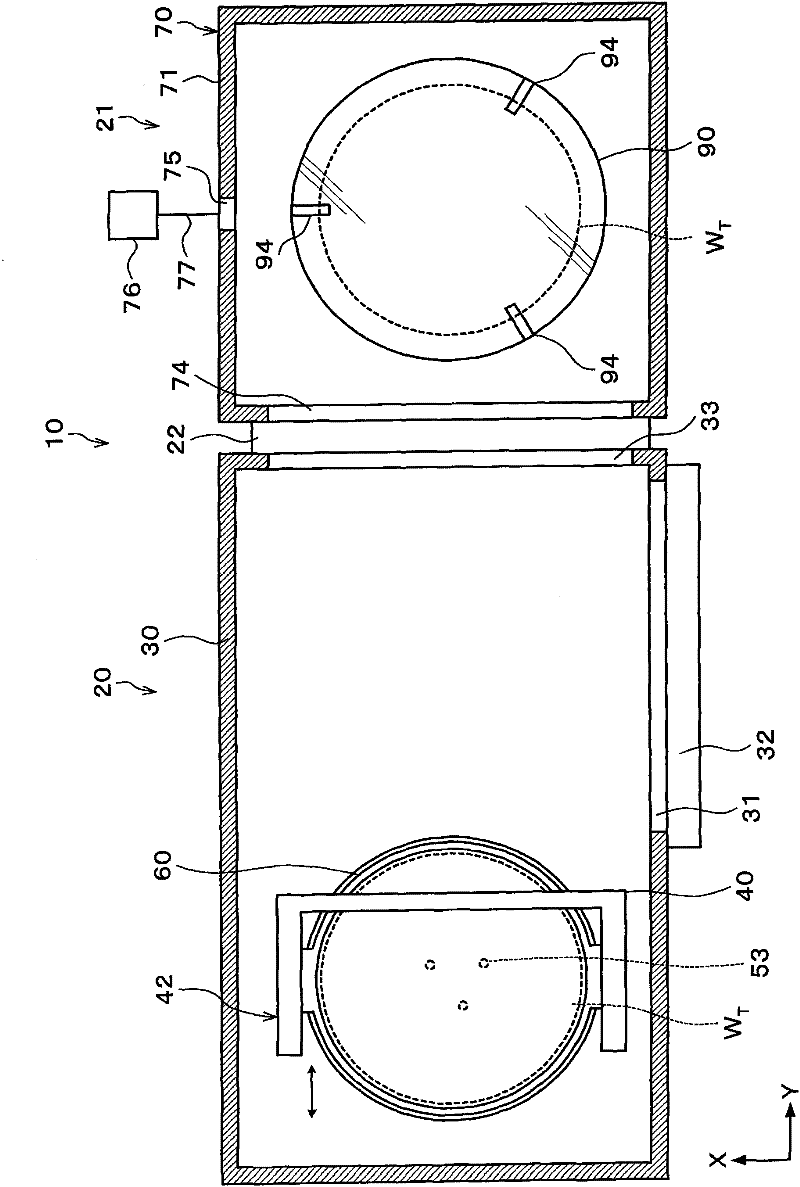
[0040] Embodiments of the present invention will be described below. figure 1 It is a longitudinal sectional view showing a schematic configuration of a joining device 10 having a pressing adapter 1 . figure 2 It is a cross-sectional view showing a schematic configuration of the joining device 10 having the pressing attachment 1 .
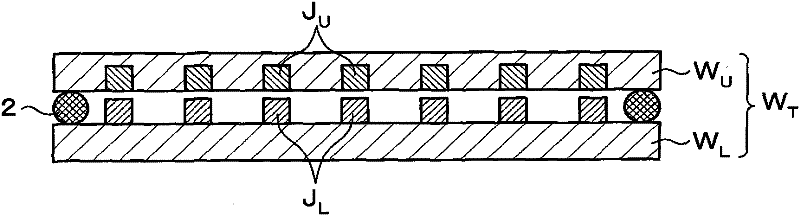
[0041] In the joining device 10, such as image 3 As shown, for example, two wafers W as substrates U , W L join together. Hereinafter, the wafer disposed on the upper side may be referred to as "upper wafer W U ", the wafer configured on the lower side is called "lower wafer W L ". Each wafer W U , W L Joints J each having a plurality of metals U 、J L . And, make each joint J U 、J L abutment so that the wafer W U , W L stacked to form a stacked wafer W as a stacked substrate T , and then the wafer W U , W L join each other. In addition, during the wafer W U , W L state before engagement of each other, such as image 3 shown i...
PUM
 Abstract
Description
Claims
Application Information