Memory structure

A memory and composite structure technology, applied in the field of split-gate flash memory structure, can solve the problem of device programming voltage reduction and achieve the effect of avoiding over-erasing and reducing the area

Active Publication Date: 2012-05-16
SHANGHAI HUAHONG GRACE SEMICON MFG CORP
View PDF3 Cites 11 Cited by
  • Summary
  • Abstract
  • Description
  • Claims
  • Application Information

AI Technical Summary

Problems solved by technology

When traditional flash memory is moving towards higher storage density, due to structural limitations, it will face great challenges to further reduce the programming voltage of the device

Method used


Image

  • Memory structure
  • Memory structure
  • Memory structure

Examples


no. 2 Embodiment approach

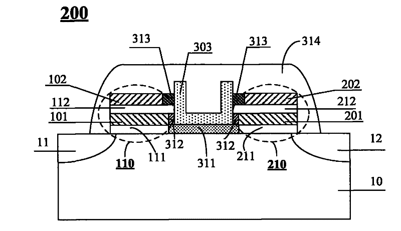
[0040] figure 2 It is a structural schematic diagram of the second specific embodiment of the memory structure provided by the present invention.

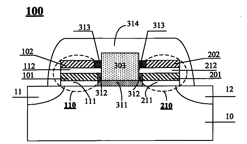
[0041] Such as figure 2 As shown, the memory structure 200 provided in this specific embodiment includes: a semiconductor substrate 10 having a first active region 11 and a second active region 12 arranged at intervals thereon; a word line 303 located on the upper surface of the semiconductor substrate 10 , between the first active region 11 and the second active region 12; the first storage bit cell 110 is located between the word line 303 and the first active area 11; the second storage bit cell 210 is located between the word line 303 and the Between the second active region 12; wherein: the first storage bit cell 110 has a first floating gate 101 and a first control gate 102, and the first control gate 102 is arranged on the first floating gate 101 at intervals; the second The storage bit unit 210 has a second floating gate...


PUM


Abstract

The invention discloses a memory structure which comprises two memory bit units and a word line positioned between the two memory bit units, wherein the two memory bit units are respectively provided with a floating gate and a control gate; the control gates are arranged above the floating gates at intervals; a tunneling oxide layer is arranged between the floating gates and the word line and is used for separating the floating gates and the word line; and a gate oxide layer is arranged between the word line and a semiconductor substrate and is used for separating the word line and the semiconductor substrate. In the memory structure, the two memory bit units share the same word line, thus the memory bit units are read, programmed and erased through applying different working voltages to the word line, the two control gates and source drain regions, the structure of the shared word line enables a gate-type flash memory to be used for reducing the area of a chip effectively under the condition that the electricity insulation performance of the chip is maintained to be changed.

Description

technical field [0001] The invention relates to a memory structure, in particular to a split-gate flash memory structure, and belongs to the technical field of semiconductors. Background technique [0002] Flash memory has become a research hotspot in non-volatile memory due to its convenience, high storage density, and good reliability. Since the first flash memory product came out in the 1980s, with the development of technology and the storage needs of various electronic products, flash memory has been widely used in mobile and communication devices such as mobile phones, notebooks, handheld computers and U disks. , flash memory is a kind of non-volatile memory. Its operating principle is to control the switch of the gate channel by changing the critical voltage of the transistor or memory cell to achieve the purpose of storing data, so that the data stored in the memory will not be lost due to power interruption. Disappears, and flash memory is a special structure of el...

Claims


Application Information

Patent Timeline
Patent Type & Authority Applications(China)
IPC IPC(8): H01L27/115H01L29/423
Inventor 顾靖
Owner SHANGHAI HUAHONG GRACE SEMICON MFG CORP
Why Eureka
Try Eureka