Multilayer inductor

An inductor and multilayer technology, applied in the field of multilayer inductors, can solve problems such as poor DC superposition characteristics

Inactive Publication Date: 2012-05-23
TAIYO YUDEN KK
View PDF5 Cites 6 Cited by
  • Summary
  • Abstract
  • Description
  • Claims
  • Application Information

AI Technical Summary

Problems solved by technology

However, conventional multilayer inductors have a problem of inferior DC superposition characteristics compared to wound inductors

Method used


Image

  • Multilayer inductor
  • Multilayer inductor
  • Multilayer inductor

Examples


no. 1 approach

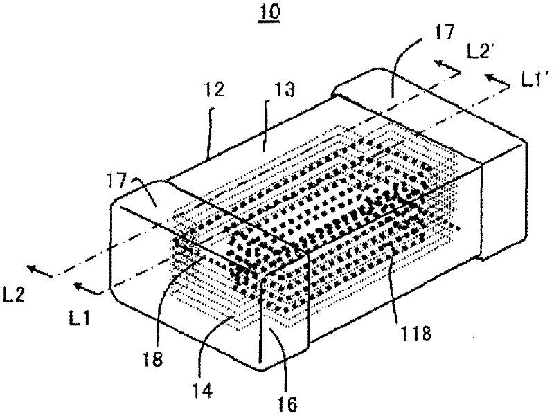
[0058] The first embodiment of the present invention is shown in Figure 1~3 . figure 1 is a stereogram, figure 2 is a cross-sectional view, figure 2 (a) is figure 1 Sectional view of L1-L1′, figure 2 (b) is figure 1 Sectional view of L2-L2′. image 3 yes figure 1 Elementary configuration diagram of the laminate chip shown.

[0059] The first embodiment of the multilayer inductor of the present invention is as follows figure 1 , image 3 As shown, a rectangular parallelepiped-shaped laminate chip 12 and a pair of external electrodes 17 formed on the end faces of the laminate chip are included.

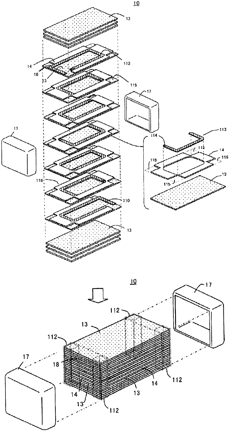
[0060] Specifically, the laminated body chip 12 includes a plurality of magnet layers 13 having a rectangular planar shape and being laminated in the thickness direction, and a plurality of coil patterns 113 arranged between adjacent magnet layers. The coil patterns 113 are connected to each other to form a helical coil 118 . Further, the coil conductor 15 is formed ...

no. 2 approach

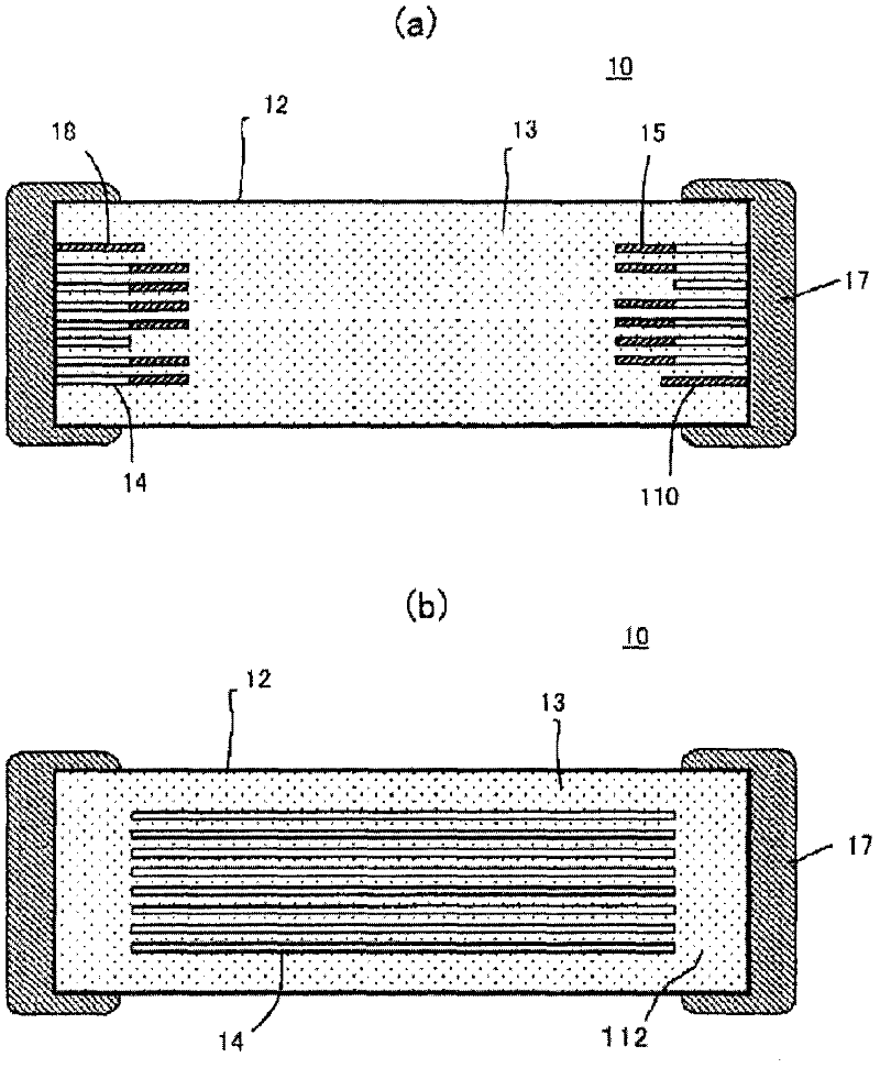
[0063] The second embodiment of the present invention is shown in Figure 4 .

[0064] A second embodiment of the multilayer inductor of the present invention is as Figure 4 As shown, a rectangular parallelepiped-shaped laminate chip 12 and a pair of external electrodes 17 formed on the end faces of the laminate chip are included.

[0065] Specifically, the laminated body chip 12 has a plurality of magnet layers 13 having a rectangular planar shape and are laminated in the thickness direction, and a plurality of coil patterns 113 respectively arranged between adjacent magnet layers. The coil patterns 113 are connected to each other to form a helical coil. Moreover, the lead-out part 18,110 which reaches the edge part of a magnetic body layer is connected to the start end and the terminal end of this coil, and the coil conductor is formed. Then, the non-magnetic layer 14 is arranged in the area outside the helical coil between layers of the adjacent magnetic layers 13 in th...

Embodiment 1

[0083] First, ethyl cellulose and terpineol were added to the FeO 2 , CuO, ZnO, NiO as the main material and the Ni-Zn-Cu series ferrite fine powder after calcining and crushing are kneaded to make a slurry. The slurry is applied to a certain thickness with a doctor blade, and the dried slurry is cut into a specific size for printing to form a magnet sheet. Through-holes are formed at specific positions on the magnet sheet by methods such as die-drilling or laser machining perforation. The silver paste was then printed onto the magnet sheet using a screen having the shape of a part of the coil pattern and dried. Non-magnetic slurry is to add ethyl cellulose, terpineol to FeO 2 , CuO, ZnO as the main material and made by mixing and kneading Zn-Cu ferrite fine powder after calcining and crushing. Screen printing was performed by positioning the non-magnetic paste to be printed on a specific position outside the coil pattern. At this time, the printed pattern shape of the non...


PUM


Abstract

Provided is a multilayer inductor which can increase the inductance value (L) and can prevent the Q-value from decreasing without losing direct current superposition characteristics. The multilayer inductor (10) has a multilayer chip (12) shaped like a rectangular parallelepiped, and a pair of external electrodes (17) formed on the end surfaces of the multilayer chip. The multilayer chip is provided with a plurality of magnetic layers (13), coil conductors (15), and nonmagnetic layers (14). Each nonmagnetic layer is provided between adjacent magnetic layers, rectangular notched portions (115) are formed at four corners of the outer periphery of each nonmagnetic layer in the outside area of a spiral coil (118), and columnar areas (112) consisting of magnetic layers are formed at the notched portions. This structure introduces magnetic flux to the columnar areas, so magnetic saturation tends not to occur, and the direct current superposition characteristics are not lost. Further, the notched portions to be formed on the nonmagnetic material are disposed so as to be brought into contact with the external electrodes, so the Q-value is improved.

Description

technical field [0001] The present invention relates to a multilayer inductor used, for example, as a choke coil of a power supply circuit or the like. Background technique [0002] For example, if Figure 12 As shown in ((a): perspective view, (b): cross-sectional view of L5-L5' in (a), the laminated inductor 29 includes a laminated chip 22 and an end face formed on the laminated chip 22. A pair of external electrodes 27 . Laminate chip 22 such as Figure 13 As shown in the component configuration diagram, the planar shape includes a plurality of magnet layers 23 stacked in the thickness direction and a plurality of coil patterns 213 arranged between adjacent magnet layers 23 and 23 . The coil patterns 213 are connected to each other to form a helical coil 218 . Furthermore, the lead-out part which reaches the edge part of the magnetic body layer 23 is connected to the start end and the terminal end of this coil 218, and the coil conductor is formed. And, if Figure 12 ...

Claims


Application Information

Patent Timeline
IPC IPC(8): H01F17/00H01F17/04
CPCH01F17/0013H01F2017/0066H01F17/00H01F17/04
Inventor 野木谦一郎上山义明冈部健次小原将孝
Owner TAIYO YUDEN KK
Why Eureka
Try Eureka