Optical sensor, semiconductor device, and liquid crystal panel

A light sensor and semiconductor technology, applied in the field of light sensors, can solve the problems of not being able to detect changes in light

Inactive Publication Date: 2012-05-23
SHARP KK
View PDF4 Cites 11 Cited by
  • Summary
  • Abstract
  • Description
  • Claims
  • Application Information

AI Technical Summary

Problems solved by technology

Therefore, there is a problem that the useful light sensor cannot detect the change of the light

Method used


Image

  • Optical sensor, semiconductor device, and liquid crystal panel
  • Optical sensor, semiconductor device, and liquid crystal panel
  • Optical sensor, semiconductor device, and liquid crystal panel

Examples


Embodiment approach 1

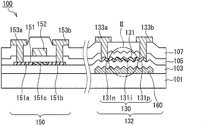
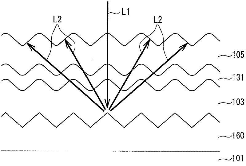
[0044] figure 1 is a cross-sectional view showing a schematic configuration of the semiconductor device 100 according to Embodiment 1 of the present invention. The semiconductor device 100 includes: a substrate 101, a thin film diode 130 formed on the substrate 101 with a base layer 103 as an insulating layer interposed therebetween, a light sensor 132 having a light shielding layer 160 provided between the substrate 101 and the thin film diode 130, and a thin film Transistor 150. The substrate 101 is preferably light-transmitting. exist figure 1 In order to simplify the drawing, only a single photosensor 132 and a single thin film transistor 150 are shown, but a plurality of photosensors 132 and a plurality of thin film transistors 150 can be formed on a common substrate 101 . In addition, in figure 1 In the figure, for easy understanding, a cross-sectional view of the photosensor 132 and a cross-sectional view of the thin film transistor 150 are shown in the same draw...

Embodiment approach 2

[0081] In Embodiment 2, a liquid crystal panel including a semiconductor device having the photodetection function described in Embodiment 1 will be described.

[0082] Figure 4 It is a cross-sectional view showing a schematic configuration of a liquid crystal display device 500 including a liquid crystal panel 501 according to the second embodiment.

[0083] The liquid crystal display device 500 includes: a liquid crystal panel 501 ; an illuminating device 502 for illuminating the backside of the liquid crystal panel 501 ;

[0084] The liquid crystal panel 501 includes: a TFT array substrate 510 and an opposing substrate 520 , both of which are light-transmitting plate-like members; and a liquid crystal layer 519 sealed between the TFT array substrate 510 and the opposing substrate 520 . Materials for forming the TFT array substrate 510 and the counter substrate 520 are not particularly limited. For example, the same materials as those used in conventional liquid crystal p...


PUM

PropertyMeasurementUnit
thicknessaaaaaaaaaa
thicknessaaaaaaaaaa
thicknessaaaaaaaaaa

Abstract

Disclosed are an optical sensor, a semiconductor device, and a liquid crystal panel wherein a thin-film diode has improved optical detection sensitivity and a semiconductor layer thereof has improved light-use efficiency, even if the semiconductor layer is thin. One side of a substrate (101) is provided with a thin-film diode (130) having a first semiconductor layer (131) containing an n-type region (131n) and a p-type region (131p), at least. A light-blocking layer (160) is provided between the substrate and the first semiconductor layer. Surface asperities are formed on the side of the light-blocking layer that faces the first semiconductor layer, and the first semiconductor layer has a texture that matches the surface asperities of the light-blocking layer. Light incident on the light-blocking layer is diffusely reflected into the first semiconductor layer. Since the first semiconductor layer has a texture that matches the surface asperities of the light-blocking layer, the distance the diffusely-reflected light travels in the first semiconductor layer is increased. As a result, the amount of light absorbed by the first semiconductor layer increases and the optical detection sensitivity improves.

Description

technical field [0001] The present invention relates to an optical sensor including a thin film diode (TFD) having a semiconductor layer including at least an n-type region and a p-type region. In addition, the present invention also relates to a semiconductor device including a thin film diode and a thin film transistor (Thin Film Transistor: TFT). Furthermore, the present invention also relates to a liquid crystal panel including the semiconductor device. Background technique [0002] A touch sensor function can be realized by installing a light sensor including a thin film diode in a display device. In such a display device, touching the observer-side surface (that is, the display surface) of the display device with a finger or a stylus changes the incident light from the display surface side, and the incident light is detected by an optical sensor. Changes to enable information input. [0003] In such a display device, there is little change in light caused by touchin...

Claims


Application Information

Patent Timeline
Patent Type & Authority Applications(China)
IPC IPC(8): H01L31/10G02F1/1333G02F1/1335G02F1/136G09F9/30H01L27/14H01L29/786
CPCG02F1/13338G06F2203/04103G06F3/0421H01L27/14678H01L31/0236H01L31/105H01L31/02164H01L27/1214Y02E10/50H01L27/14692G06F3/0412H01L31/02363
Inventor 织田明博中泽淳
Owner SHARP KK
Why Eureka
Try Eureka