Gate forming method

A gate and dummy gate technology, used in electrical components, semiconductor/solid-state device manufacturing, semiconductor devices, etc., can solve problems such as substrate damage, and achieve the effect of reducing voids, avoiding the formation of voids, and avoiding damage

Active Publication Date: 2014-06-04
SEMICONDUCTOR MANUFACTURING INTERNATIONAL (BEIJING) CORP
View PDF7 Cites 0 Cited by
  • Summary
  • Abstract
  • Description
  • Claims
  • Application Information

AI Technical Summary

Problems solved by technology

However, in this patent document, the argon (Ar) sputtering process is used to increase the width of the top of the trench, which is easy to cause damage to the substrate

Method used


Image

  • Gate forming method
  • Gate forming method
  • Gate forming method

Examples


Embodiment Construction

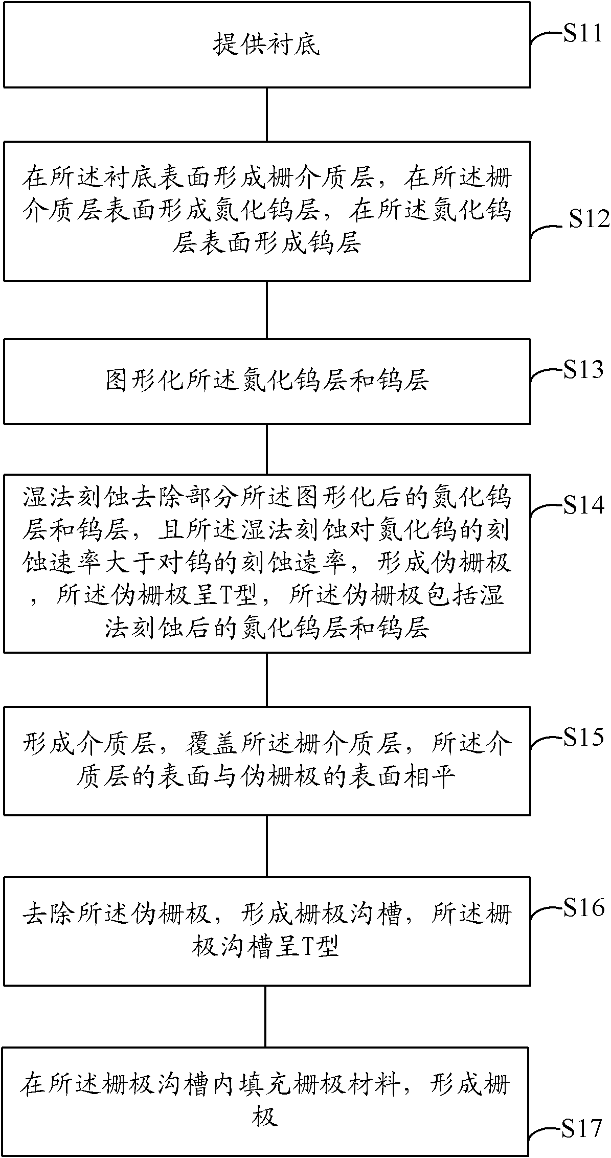
[0029] After long-term research, the inventor hopes to find a simple process to form a gate trench with a width at the top greater than that at the bottom, which is conducive to the filling of the gate material and avoids the formation of voids, or at least reduces the formation of voids; moreover, it can avoid the existing There is the disadvantage of causing damage to the substrate as described in the art. After reading a lot of materials, the inventor unexpectedly discovered that the article "resist removal and cleaning for TANOS metal Gate on volatile memories" discloses that when wet etching tungsten nitride and tungsten, the etching rate of tungsten nitride is greater than that of tungsten.

[0030] In the method for forming a grid in a specific embodiment of the present invention, when etching tungsten nitride and tungsten by a wet method, the etching rate of tungsten nitride is higher than that of tungsten, and a patterned grid is formed on the substrate. The tungsten...


PUM


Abstract

The invention discloses a gate forming method comprising the following steps: providing a substrate; forming a gate dielectric layer on the surface of the substrate, forming a tungsten nitride layer on the surface of the gate dielectric layer and forming a tungsten layer on the surface of the tungsten nitride layer; patterning the tungsten nitride layer and the tungsten layer; etching part of patterned tungsten nitride layer and tungsten layer by using a wet process, and forming a false gate, wherein the speed for etching the tungsten nitride by using the wet process is larger than the speed for etching tungsten, and the false gate is T-shaped and comprises the tungsten nitride layer and the tungsten layer which are etched by using the wet process; forming a dielectric layer to cover the gate dielectric layer, wherein the surface of the dielectric layer is level with the surface of the false gate; removing the false gate to form a T-shaped gate trench; and filling gate materials in the gate trench to form a gate. The gate forming method is beneficial to filling the gate materials, and formed gaps can be avoided or at least reduced; and the method is simple, and the defect that the substrate is damaged in the prior art can be avoided.

Description

technical field [0001] The invention relates to the technical field of semiconductors, in particular to a method for forming a gate. Background technique [0002] In the prior art, the process of forming a gate can be divided into a gate first process and a gate last process. The gate-front process refers to first depositing a gate dielectric layer, forming a gate electrode on the gate dielectric layer, then performing source-drain implantation, and then performing an annealing process to activate ions in the source-drain. The process steps of the front-gate process are simple, but during annealing, the gate electrode must inevitably withstand high temperatures, resulting in a shift in the threshold voltage Vt of the MOS tube and affecting the performance of the tube. The gate last process means that after the annealing process, that is, after the high temperature step, the polysilicon dummy gate is etched away to form a dummy gate trench, and then the dummy gate trench is ...

Claims


Application Information

Patent Timeline
Patent Type & Authority Patents(China)
IPC IPC(8): H01L21/28H01L21/283H01L21/3213
Inventor 卢炯平洪中山
Owner SEMICONDUCTOR MANUFACTURING INTERNATIONAL (BEIJING) CORP
Why Eureka
Try Eureka