Unlock instant, AI-driven research and patent intelligence for your innovation.

Phase change random access memory array and formation method thereof, and phase change random access memory unit and formation method thereof

A technology of phase change memory and array, applied in the direction of electrical components, etc., can solve the problems of high cost and complex process of phase change memory, and achieve the effects of low cost, easy control, and reduced power loss

Active Publication Date: 2014-07-30
SEMICON MFG INT (SHANGHAI) CORP +1
View PDF4 Cites 0 Cited by
  • Summary
  • Abstract
  • Description
  • Claims
  • Application Information

AI Technical Summary

Problems solved by technology

However, in practical applications, it is found that the existing process of forming phase change memory is relatively complicated and the cost is high

Method used


Image

  • Phase change random access memory array and formation method thereof, and phase change random access memory unit and formation method thereof
  • Phase change random access memory array and formation method thereof, and phase change random access memory unit and formation method thereof
  • Phase change random access memory array and formation method thereof, and phase change random access memory unit and formation method thereof

Examples


Embodiment Construction

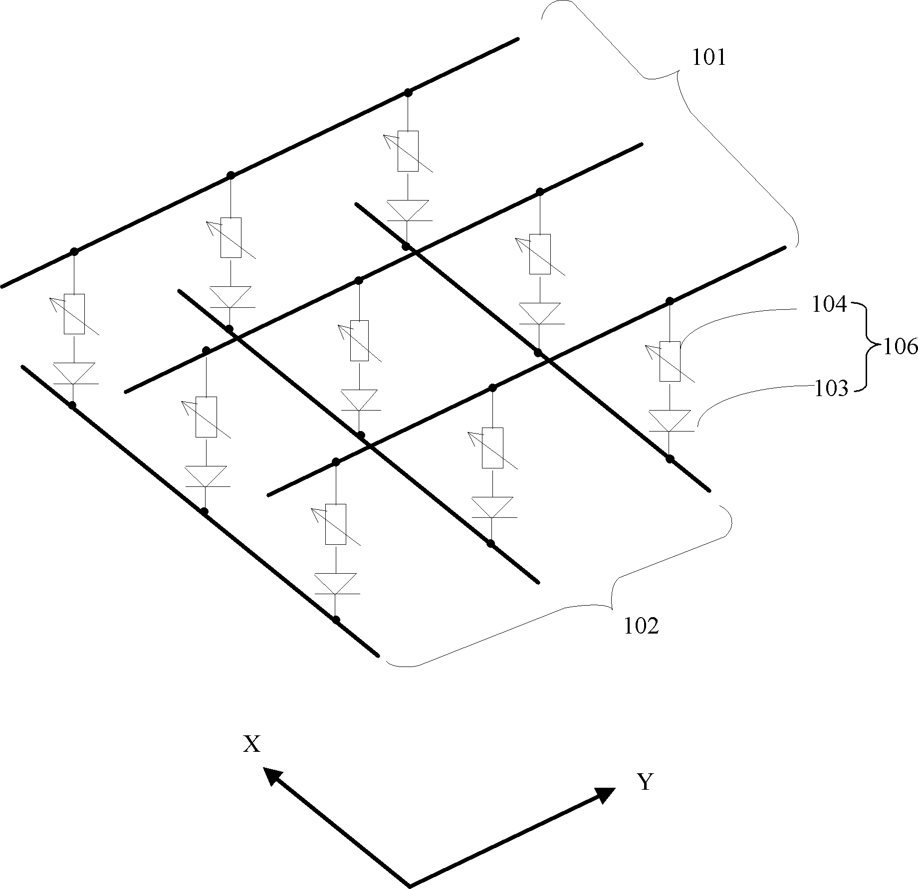
[0045] The present invention embeds the word line by forming a low-resistance conductive region in the semiconductor substrate. Compared with the existing technology of forming a phase-change memory array, the process is simple and compatible with the CMOS process, and the cost is low; further, the present invention In the embodiment of the invention, the resistivity of the word line formed by implantation or diffusion is low, which can reduce the power loss of the overall phase change memory; furthermore, the embodiment of the invention forms a third semiconductor doped area, which can reduce the crosstalk between adjacent phase change memory cells.

[0046] In order to achieve the above object, the present invention firstly provides a method for forming a phase change memory array, comprising: providing a semiconductor substrate; forming a diode array on the semiconductor substrate, the diode array including diodes arranged in a row direction and a column direction, Differen...


PUM


Abstract

The invention relates to a phase change random access memory (PCRAM) unit that comprises a semiconductor substrate and diodes. Each of the diodes includes: a first doped semiconductor region, which has a first conductive type and is arranged on the semiconductor substrate; and a conductive region, which is covered on the first doped semiconductor region; and the conductive region and the first doped semiconductor region form a diode. Besides, the PCRAM also comprises a low-resistance conductive region that is arranged in the semiconductor substrate and is electrically connected with the first doped semiconductor regions of the diodes. In addition, the invention also provides a formation method of the PCRAM unit, a PCRAM array and a formation method thereof. According to the invention, word lines are formed and embedded by forming a low-resistance conductive region in the semiconductor substrate; compared with a current technology for forming a PCRAM array, the provided method for forming a PCRAM array has a simple process and is compatible with the CMOS technology; and cost is low.

Description

technical field [0001] The invention relates to the field of semiconductor technology, in particular, the invention relates to a phase-change memory array, a phase-change memory unit and a forming method thereof. Background technique [0002] Phase Change Random Access Memory (PCRAM) technology is based on the idea that S.R. Ovshinsky proposed in the late 1960s that phase change films could be applied to phase change storage media. As an emerging non-volatile storage technology, phase change memory has great advantages over flash memory in many aspects such as read and write speed, read and write times, data retention time, unit area, and multi-value realization. It has become the focus of current research on non-volatile storage technology. [0003] In phase change memory, the phase change material has crystalline and amorphous states. The phase change material has low resistivity when in the crystalline state and high resistivity when in the amorphous state. Because the...

Claims


Application Information

Patent Timeline
Patent Type & Authority Patents(China)
IPC IPC(8): H01L45/00
Inventor 万旭东张步新吴关平
Owner SEMICON MFG INT (SHANGHAI) CORP
Features
  • R&D
  • Intellectual Property
  • Life Sciences
  • Materials
  • Tech Scout
  • Unparalleled Data Quality
  • Higher Quality Content
  • 60% Fewer Hallucinations
Learn More