Method for preparing large-area flexible conductive film

A flexible conductive, large-area technology, applied in the field of flexible electronics, can solve the problems of poor stretchability, poor film conductivity, film cracking, etc., and achieve the effects of avoiding damage, excellent stretchability and conductivity

Inactive Publication Date: 2012-06-13
LANZHOU UNIVERSITY
View PDF3 Cites 28 Cited by
  • Summary
  • Abstract
  • Description
  • Claims
  • Application Information

AI Technical Summary

Problems solved by technology

However, the quality of the film grown at low temperature is relatively poor, resulting in poor conductivity of the film, and due to the oxide conductive film (such as: In 2 o 3 :Sn, ZnO:Al) are relatively brittle and have poor stretchability. The substrate will crack during multiple bending and folding processes, and even the film will be separated from the substrate.

Method used


Image

  • Method for preparing large-area flexible conductive film
  • Method for preparing large-area flexible conductive film
  • Method for preparing large-area flexible conductive film

Examples


Embodiment 1

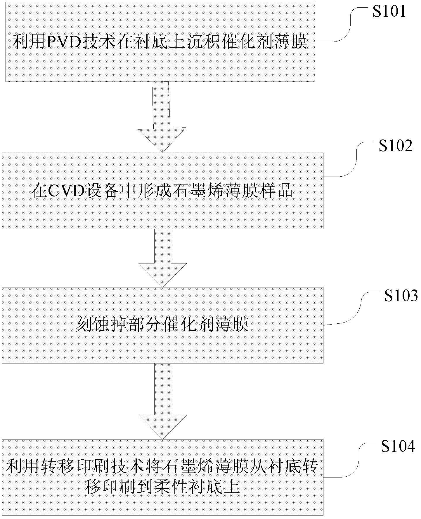
[0035] Such as figure 1 As shown, a method for preparing a large-area flexible conductive film includes the following steps: In step 101, a layer of SiO is formed on the Si sheet 2 Form the substrate, and use PVD technology to deposit a catalyst film on the substrate;

[0036] In step 102, the substrate on which the catalyst thin film is deposited is placed in a CVD device, and a large flow of Ar and H 2 gas, while rapidly raising the CVD temperature to 800°C, and then passing CH 4 Gas, after a few minutes, close the CH 4 The gas valve quickly cooled the CVD equipment to room temperature, and obtained the graphene film sample;

[0037] In step 103, the graphene film sample is placed in an etchant, and part of the catalyst film is etched away;

[0038] In step 104, the graphene film is transferred from the substrate to the flexible substrate by transfer printing technology.

[0039] Among them: PVD technology is electron beam evaporation or sputtering. The catalyst is Ni ...

Embodiment 2

[0047] In step 102 of Embodiment 1, the substrate on which the catalyst thin film is deposited is placed in a CVD device, and a large flow of Ar and H 2 gas while rapidly raising the CVD temperature to 900°C.

Embodiment 3

[0049] In step 102 of Embodiment 1, the substrate on which the catalyst thin film is deposited is placed in a CVD device, and a large flow of Ar and H 2 gas, while rapidly raising the CVD temperature to 1000°C.


PUM


Abstract

The invention discloses a method for preparing a large-area flexible conductive film, which includes the following steps: generating a SiO2 layer on a Si sheet to form a substrate and depositing a catalyst film on the substrate by using the physical vapor deposition (PVD) technology; placing the substrate deposited with the catalyst film in a chemical vapor deposition (CVD) device, introducing large flow Ar gas and H2 gas, simultaneously quickly heating the CVD device to 800 DEG C-1100 EDG C, introducing CH4 gas continuously for a few minutes, closing a CH4 air valve, and cooling the CVD device fast to room temperature to obtain a graphene film sample; placing the graphene film sample into etchant to etch away partial catalyst film; and transfer printing the graphene film sample to a flexible substrate from the substrate by using the transfer printing technology. The method achieves the purpose of preparing the large-area flexible conductive film which is good in conductive performance and capable of being folded and bent, and simultaneously can avoid damage to the flexible substrate caused by high temperature environment during preparing.

Description

technical field [0001] The invention relates to the field of flexible electronics, in particular to a method for making a large-area flexible conductive film using graphene. Background technique [0002] Traditional electronic devices are usually prepared on hard flat substrate materials, but with the advancement of technology, people began to try to develop flexible electronic devices (flexible light-emitting diodes, flexible solar cells, flexible displays, electronic eyes, etc.), which gradually produced A new discipline, flexible electronics. As an important part of the subject research, flexible conductive films have attracted a lot of attention. Initially, the research object of flexible conductive thin films mainly focused on organic semiconducting materials, but even the best organic single crystal materials still have a mobility of 1-2 cm 2 / (V s) (n-type semiconductor), 10-20 cm 2 / (V s) (p-type semiconductor), far from being comparable to the inorganic semicondu...

Claims


Application Information

Patent Timeline
Patent Type & Authority Applications(China)
IPC IPC(8): H01B13/00H01L21/02
Inventor 兰伟朱承泉李育仁苏庆谢二庆
Owner LANZHOU UNIVERSITY
Why Eureka
Try Eureka