Method for manufacturing printed circuit board (PCB) with step-shaped grooves

A technology of PCB boards and manufacturing methods, which is applied in the fields of printed circuit manufacturing, electrical components, printed circuits, etc., can solve the problems of complex manufacturing process, long cycle, unfavorable batch production, etc., and achieve the effect of high efficiency and simple manufacturing process

Active Publication Date: 2012-06-13
DONGGUAN SHENGYI ELECTRONICS
View PDF3 Cites 23 Cited by
  • Summary
  • Abstract
  • Description
  • Claims
  • Application Information

AI Technical Summary

Problems solved by technology

This kind of method has complex manufacturing process, long cycle, low production efficiency, is not conducive to mass production, and requires manual operation (putting in gaskets). The gasket discharge accuracy (key f

Method used


Image

  • Method for manufacturing printed circuit board (PCB) with step-shaped grooves
  • Method for manufacturing printed circuit board (PCB) with step-shaped grooves
  • Method for manufacturing printed circuit board (PCB) with step-shaped grooves

Examples


Embodiment Construction

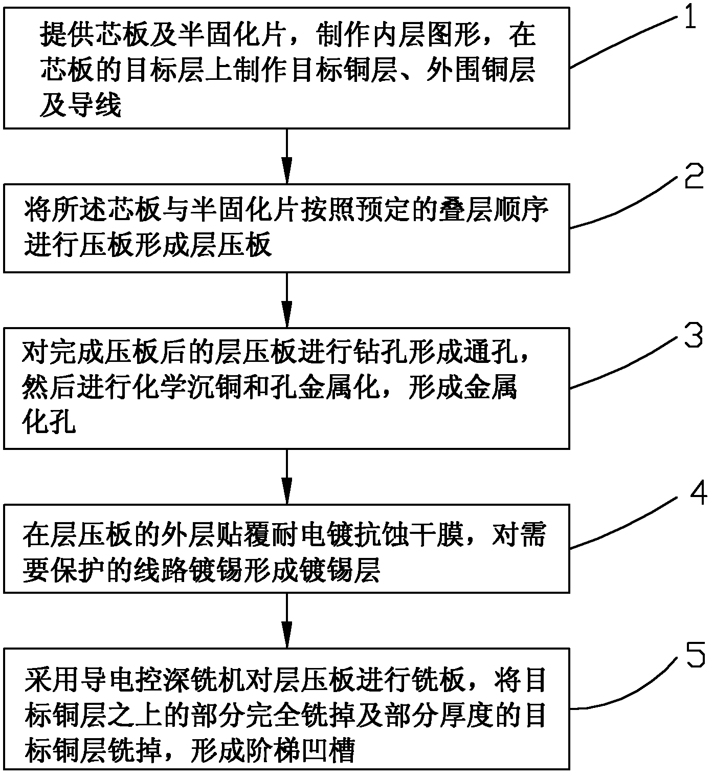
[0022] Such as Figure 1 to Figure 7 Shown, the manufacturing method of the PCB board of tool stepped groove of the present invention, comprises the following steps:

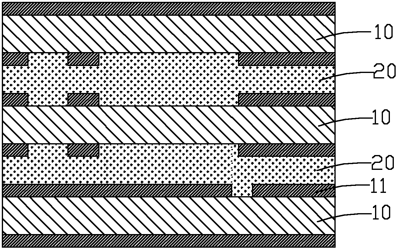
[0023] Step 1: Provide a core board 10 and a prepreg 20, and make an inner layer pattern on the core board 10, one of the core boards 10 has a target layer 11 corresponding to the bottom of the stepped groove 13 to be made, in the A target copper layer 111 is made on the target layer 11 corresponding to the position of the stepped groove 13 to be made, and a peripheral copper layer 112 and a wire 113 are made on the target layer 11 on the periphery of the target copper layer 111. Layer 112 is spaced from the target copper layer 111 and connected to the target copper layer 111 by wire 113, the structure of the target layer 11 is as follows Figure 6 shown;

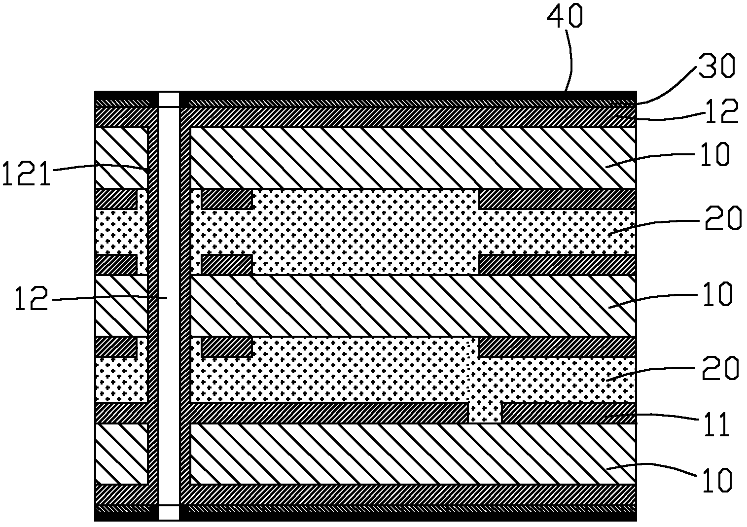
[0024] Step 2: Press the core board 10 and the prepreg 20 according to a predetermined stacking sequence to form a laminated board. The structure of the la...


PUM


Abstract

The invention relates to a method for manufacturing a printed circuit board (PCB) with step-shaped grooves. The method comprises the following steps of: 1, providing core plates and prepregs, preparing an inner-layer image and preparing a target copper layer, a peripheral copper layer and wires on a target layer of one of the core plates; 2, pressing the plates to form a laminated plate; 3, drilling to form a through hole and then performing chemical copper deposition and hole plating so as to form a plated hole which is connected with the peripheral copper layer of the target layer; 4, gluing an electroplating-and-corrosion-resisting dry film and tinning to form a tin coating; and 5, milling the laminated plate by an electricity-conducting depth-controllable milling machine to ensure that all parts on the target copper layer and part of the target copper layer are milled off and the step-shaped grooves are formed. Through the method for manufacturing the PCB with the step-shaped grooves, the target copper layer is prepared on the target layer and is connected with the superficial tin coating, and the plates are milled by the electricity-conducting depth-controllable milling machine to ensure that the milling depth can be effectively controlled, the manufacturing process is simple and is high in efficiency, and the method is suitable for batch production.

Description

technical field [0001] The invention relates to the field of manufacturing printed circuit boards, in particular to a method for manufacturing a PCB board with stepped grooves. Background technique [0002] At present, for the production of stepped groove printed circuit boards (PCBs) with small size and the specified dielectric layer must be controlled not to be damaged, it is mainly produced by embedding buffer resist gaskets and then slotting. This kind of method has complex manufacturing process, long cycle, low production efficiency, is not conducive to mass production, and requires manual operation (putting in gaskets). The gasket discharge accuracy (key factor for glue flow control) is affected by the size and number of step grooves and the operation Due to the limitation of personnel skills and other factors, it is difficult to ensure the stable and controlled flow of glue in the step groove. Contents of the invention [0003] Therefore, the object of the present ...

Claims


Application Information

Patent Timeline
IPC IPC(8): H05K3/00
Inventor 焦其正唐海波杜红兵辜义成曾志军
Owner DONGGUAN SHENGYI ELECTRONICS
Why Eureka
Try Eureka