Optical microcavity biochemical sensor
A biochemical sensor and optical microcavity technology, applied in the field of optical sensing, can solve the problems of demanding sensor technology and achieve the effects of process compatibility, lower process requirements, and low resolution requirements
- Summary
- Abstract
- Description
- Claims
- Application Information
AI Technical Summary
Problems solved by technology
Method used
Image
Examples
Embodiment 1
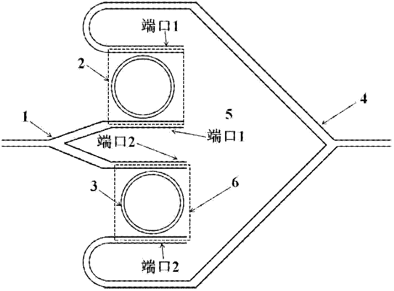
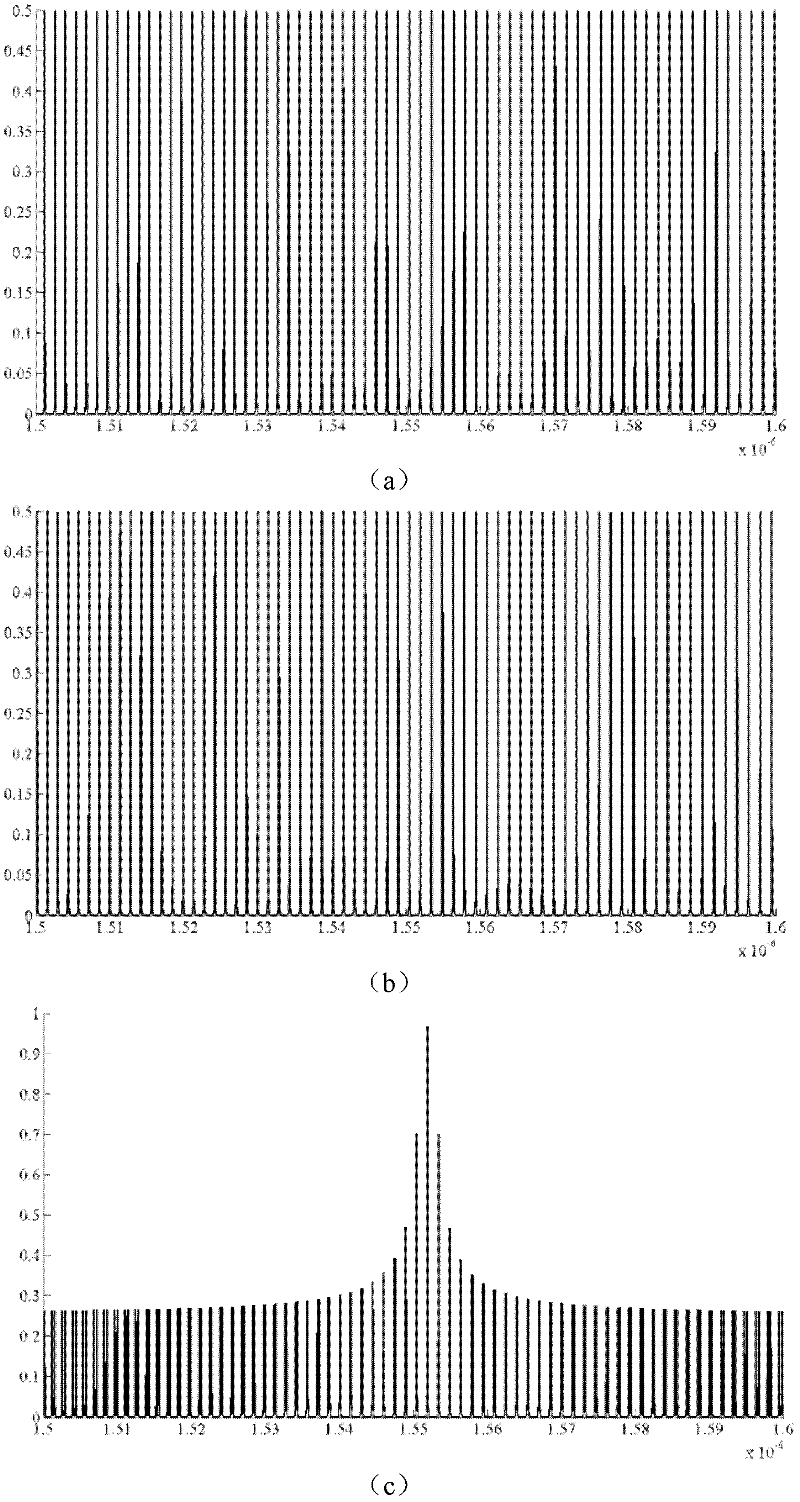
[0040] refer to figure 1 , the present invention is a high-sensitivity sensor based on the coupling of a 3dB optical beam splitter and an optical microring, comprising a first 3dB optical beam splitter 1, a second 3dB optical beam splitter 4, a sensing microring 2, A reference microring 3 , a sample well 5 and a reference well 6 . Wherein the sensing microring 2 is located in the sample groove 5 , and the reference microring 3 is located in the reference groove 6 . The incident light is input by the first 3dB optical beam splitter 1, and is coupled with the sensing microring 2 and the reference microring 3 after beam splitting; the light coupled into the sensing microring 2 and the reference microring 3 is respectively coupled with the second The straight waveguides on both sides of the 3dB optical beam splitter 4 are coupled to each other, and are output as sensing signals after interference. Taking the SOI material as an example, the cross-sectional size of the waveguide i...
Embodiment 2
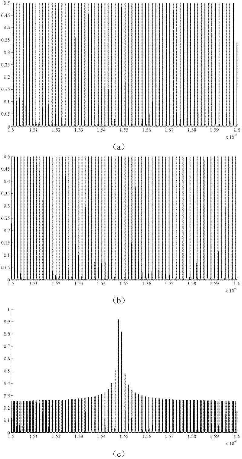
[0062] refer to figure 1 , the present invention is a high-sensitivity sensor based on the coupling of a 3dB optical beam splitter and an optical microring, comprising a first 3dB optical beam splitter 1, a second 3dB optical beam splitter 4, a sensing microring 2, A reference microring 3 , a sample well 5 and a reference well 6 . Wherein the sensing microring 2 is located in the sample groove 5 , and the reference microring 3 is located in the reference groove 6 . The incident light is input by the first 3dB optical beam splitter 1, and is coupled with the sensing microring 2 and the reference microring 3 after beam splitting; the light coupled into the sensing microring 2 and the reference microring 3 is respectively coupled with the second The straight waveguides on both sides of the 3dB optical beam splitter 4 are coupled to each other, and are output as sensing signals after interference. Taking the SOI material as an example, the cross-sectional size of the waveguide i...
PUM
| Property | Measurement | Unit |
|---|---|---|
| radius | aaaaa | aaaaa |
| radius | aaaaa | aaaaa |
| refractive index | aaaaa | aaaaa |
Abstract
Description
Claims
Application Information


