Device for converting substrate integrated waveguide to coaxial waveguide

A substrate-integrated waveguide and coaxial waveguide technology, applied in the direction of connection devices, waveguide devices, electrical components, etc., can solve the problems of increased insertion loss, waste of resources, miniaturization resistance, etc., to achieve small device size, easy assembly and disassembly , the effect of low loss conversion

Inactive Publication Date: 2012-06-20
UNIV OF ELECTRONICS SCI & TECH OF CHINA
View PDF3 Cites 16 Cited by
  • Summary
  • Abstract
  • Description
  • Claims
  • Application Information

AI Technical Summary

Problems solved by technology

The conversion from existing substrate integrated waveguide to coaxial is through the transition of substrate integrated waveguide-microstrip line-coaxial pressure line. The addition of microstrip line not only cau

Method used


Image

  • Device for converting substrate integrated waveguide to coaxial waveguide
  • Device for converting substrate integrated waveguide to coaxial waveguide
  • Device for converting substrate integrated waveguide to coaxial waveguide

Examples


specific Embodiment 1

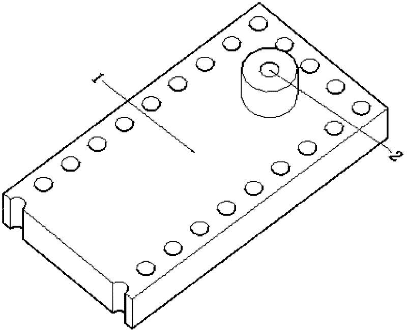
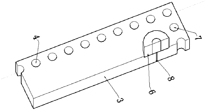
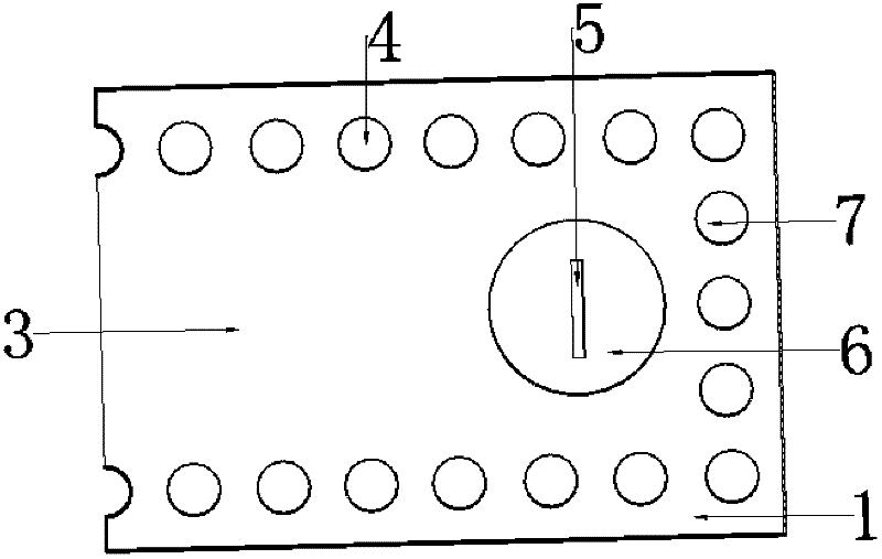
[0019] combine figure 1 and image 3 , taking the X-band as an example, the thickness of the dielectric substrate 3 of the substrate-integrated waveguide joint 1 is 3mm, the diameter of the two rows of metallized through-holes 4 is 0.4mm, and the distance between adjacent holes of each row of metallized through-holes 4 is 1.9mm , the distance between two rows of metallized through holes 4 is 22mm, the wide side of the dielectric substrate 3 is 24mm, the size of the rectangular groove 5 is 1.6mm×0.1mm, and the depth is 2.9mm; the diameter of the metal short circuit hole 7 is 0.4mm , the hole spacing is 2mm, and the diameter of the circular window 6 is 7mm. The cross-sectional size of the sheet probe 8 at the front end of the coaxial inner conductor of the coaxial waveguide joint 2 is 1.6 mm×0.1 mm, and the length of the probe is 2.9 mm. The coaxial cable of the coaxial waveguide connector 2 is a 50Ω standard coaxial cable, the diameter of the inner conductor is 3.04mm, and t...

specific Embodiment 2

[0021] combine figure 2 and image 3 , taking the X-band as an example, the thickness of the dielectric substrate 3 of the substrate-integrated waveguide connector 1 is 3mm, the diameter of the two rows of metallized through-holes 4 is 0.5mm, and the distance between adjacent holes in each row of metallized through-holes 4 is 1.9mm , the distance between two rows of metallized through holes 4 is 22mm, the wide side of the dielectric substrate 3 is 23.56mm, the size of the rectangular groove 5 is 1.6mm×0.1mm, and the depth is 2.9mm; the diameter of the metal short circuit hole 7 is 0.5 mm, the hole spacing is 2mm, and the diameter of the circular window 6 is 7mm. The cross-sectional size of the sheet probe 8 at the front end of the coaxial inner conductor of the coaxial waveguide joint 2 is 1.6 mm×0.1 mm, and the length of the probe is 2.9 mm. The coaxial cable of the coaxial waveguide connector 2 is a 50Ω standard coaxial cable, the diameter of the inner conductor is 3.04mm...

specific Embodiment 3

[0023] combine figure 1 and image 3 , taking the X-band as an example, the thickness of the dielectric substrate 3 of the substrate-integrated waveguide connector 1 is 3mm, the diameter of the two rows of metallized through-holes 4 is 0.6mm, and the distance between adjacent holes of each row of metallized through-holes 4 is 1.5mm , the distance between two rows of metallized through holes 4 is 22mm, the wide side of the dielectric substrate 3 is 23.56mm, the size of the rectangular groove 5 is 1.5mm×0.1mm, and the depth is 2.9mm, and the diameter of the metal short circuit hole 7 is 0.6 mm, the hole spacing is 1mm, and the diameter of the circular window 6 is 7mm. The slice probe 8 at the front end of the coaxial inner conductor of the coaxial waveguide connector 2 has a cross-sectional dimension of 1.5 mm×0.1 mm, and a probe length of 2.9 mm. The coaxial cable of the coaxial waveguide connector 2 is a 50Ω standard coaxial cable, the diameter of the inner conductor is 3.0...


PUM

PropertyMeasurementUnit
Insertion lossaaaaaaaaaa

Abstract

The invention discloses a device for converting substrate integrated waveguide to coaxial waveguide, belonging to the technical field of microwave and millimeter wave devices. The device comprises a substrate integrated waveguide connector and a coaxial waveguide connector; a row of short-circuit through holes are arranged in one end of the substrate integrated waveguide on which the substrate integrated waveguide connector is located to connect two metal layers; the upper metal layer of a dielectric substrate close to one end of the short-circuit through hole is provided with a round window with the size equal to the diameter of an outer conductor of the coaxial waveguide; and the circle center of the round window is located on the central axis of the substrate integrated waveguide; a rectangular groove is arranged at the center of a round dielectric substrate exposed outside the round window; the front end of an inner conductor of the coaxial waveguide connector is processed into a slice probe which is inserted into the rectangular groove; and the outer conductor of the coaxial waveguide is contacted and fixed with the upper metal layer of the dielectric substrate. The inter-conversion between substrate integrated waveguide and coaxial waveguide with low reflection and low loss is realized. The device is small in size and easy and convenient to assemble and disassemble and can be used repeatedly, which is convenient for the testing and the utilization of substrate integrated waveguide devices and systems.

Description

technical field [0001] The invention belongs to the technical field of microwave and millimeter wave devices, and relates to a connection conversion device between waveguide structures, in particular to a conversion device between a substrate integrated waveguide and a coaxial waveguide. Background technique [0002] Substrate integrated waveguide (siw) is a new type of waveguide structure, which is derived from rectangular waveguide and microstrip line, and has the advantages of low cost, low loss, high Q value, and high-density integration of microwave and millimeter wave circuits and their subsystems . SIW technology is developing rapidly, and its products include SIW filters, SIW directional couplers, SIW circulators, SIW-microstrip line adapters and other passive devices. The substrate-integrated waveguide has gradually become an important development direction of microwave transmission lines and devices. In microwave and millimeter wave systems, these devices based o...

Claims


Application Information

Patent Timeline
IPC IPC(8): H01P5/08
Inventor 陈良熊林汪晓光邓龙江梁迪飞
Owner UNIV OF ELECTRONICS SCI & TECH OF CHINA
Why Eureka
Try Eureka