
Method for measuring warpage of electronic packaging product

A technology of electronic packaging and measurement methods, applied in electromagnetic measurement devices, electric/magnetic solid deformation measurement, etc., can solve the problems of high cost, inability to warp measurement, inconvenient use, etc., and achieve the effect of cost advantage

Active Publication Date: 2015-01-21
FUDAN UNIV
View PDF3 Cites 0 Cited by
  • Summary
  • Abstract
  • Description
  • Claims
  • Application Information

AI Technical Summary

Problems solved by technology

However, this method also has application problems: first, the warpage measurement of silicon wafers needs to use a complete wafer, and it is impossible to measure the warpage of the packaged system; Cleanliness requirements are very high, and any small contamination on the silicon wafer will affect the final measurement results
In addition, this measurement method has strict requirements on ambient temperature and humidity, and it is inconvenient to use; moreover, the current cost of such instruments is still relatively high

Method used


Image

  • Method for measuring warpage of electronic packaging product
  • Method for measuring warpage of electronic packaging product
  • Method for measuring warpage of electronic packaging product

Examples


Embodiment Construction

[0032] Specific embodiments of the present invention will be described in detail below in conjunction with the accompanying drawings.

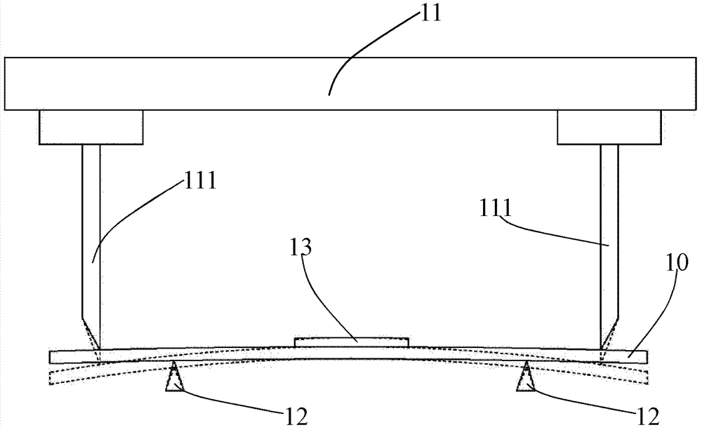
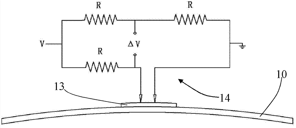
[0033] For the silicon stress sensor chip, when the chip itself is subject to a certain stress, the size of the piezoelectric resistance in the chip will change, so that the change of its stress can be obtained according to the change of its electrical parameters. Utilizing this characteristic of the silicon stress sensor, the warpage of the electronic packaging system can be quantitatively measured.

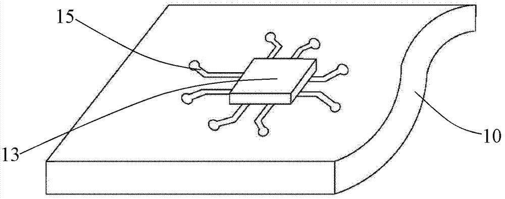
[0034] Use an adhesive to attach the silicon stress sensor chip to the surface of the product under test (such as a silicon wafer, a printed circuit board, etc.), and when the product under test warps to a certain extent, the stress sensor chip will also produce a corresponding deformation , so that in-plane normal stress and shear force are generated inside the chip. The magnitude of these additional normal stresses and shearing forces can be ...


PUM


Abstract

The invention provides a method for measuring the warpage of an electronic packaging product. The method comprises the following steps of: (1) sensor chip calibration: installing a silicon stress sensor chip on a surface of a calebration sample; using a pressing block to enable a product to be measured to be warped and deformed so that an output voltage is generated because of warpage and deformation of the silicon stress sensor chip; and calibrating the relationship of the output voltage of the silicon stress sensor chip and the warpage degree of the calebration sample according to a measurement result; (2) measurement of warpage of the electronic packaging product: installing the silicon stress sensor chip on the surface or inside the electronic packaging product to be measured; warping and deforming the sensor chip to form an output voltage; and obtaining the warpage degree of the electronic packaging product to be measured according to the calibrated relationship and the measurement result. According to the method disclosed by the technical scheme of the invention, the warpage condition in the process of packaging or in the packaging system can be monitored, thus packaging process parameters are regulated and perfected according to the measurement result.

Description

technical field [0001] The present invention relates to electronic packaging, in particular to a method for measuring the degree of warpage of electronic packaging products. Background technique [0002] In the electronic packaging system, the warpage of the silicon wafer and the printed circuit board will have a great impact on the performance of the packaging system. Using a specific method to measure the warpage of this type of system can provide useful help for improving the design and process of the packaging system. [0003] At present, the warpage of silicon wafers mainly adopts the "Non-contact Test Method for Warpage of Silicon Wafers" (national standard GB / T6620-200×), the silicon wafers are placed on the 3 fulcrums of the reference ring, and the 3 fulcrums form a benchmark flat. A pair of probes of the tester scans synchronously on the upper and lower surfaces of the silicon wafer along a prescribed path. During the scanning process, the distance between the up...

Claims


Application Information

Patent Timeline
Patent Type & Authority Patents(China)
IPC IPC(8): G01B7/16
Inventor 蒋程捷肖斐
Owner FUDAN UNIV
Learn More