Graphical test method of semiconductor devices

A test method and semiconductor technology, applied in the direction of instruments, measuring electricity, measuring devices, etc., can solve the problems of low maintainability, long development cycle, poor convenience, etc., to enhance maintainability, shorten development cycle, and develop convenience. improved effect

Inactive Publication Date: 2012-06-27
UNIV OF ELECTRONICS SCI & TECH OF CHINA
View PDF5 Cites 12 Cited by
  • Summary
  • Abstract
  • Description
  • Claims
  • Application Information

AI Technical Summary

Problems solved by technology

[0004] In the prior art, high-level languages ​​such as C / C++ / C# / Java etc. are used to write a set of special test programs for each semiconductor device. Although these high-level languages ​​are powerful and flexible, there are deficiencies in the use of the testing technology field. Disadvantage: For a semiconductor, the test program is written in a high-level language, which is poor in convenience, long in development cycle and low in maintainability

Method used


Image

  • Graphical test method of semiconductor devices
  • Graphical test method of semiconductor devices
  • Graphical test method of semiconductor devices

Examples


Embodiment Construction

[0032] Specific embodiments of the present invention will be described below in conjunction with the accompanying drawings, so that those skilled in the art can better understand the present invention. It should be noted that in the following description, when detailed descriptions of known functions and designs may dilute the main content of the present invention, these descriptions will be omitted here.

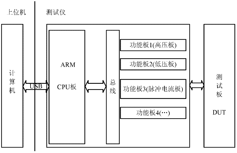
[0033] figure 1 It is a schematic block diagram of semiconductor device testing.

[0034] The semiconductor device graphical testing method of the present invention relies on a semiconductor device tester, adopts a host computer and a tester framework, makes the development environment and the operating environment independent of each other, and improves the safety and stability of the test.

[0035] Such as figure 1 As shown, the tester includes a core control board, namely the CPU board, a high-voltage board that generates high-voltage excitation, a low-voltage board th...


PUM


Abstract

The invention discloses a graphical test method of semiconductor devices. A test program is divided into a top layer, a test index layer and a programming module layer, wherein the top layer testing process is formed by test indexes; the test index layer is formed by programming modules according to a semiconductor test step; and the programming module layer corresponds to operation and needed parameters of the step. When the test program is developed, only the test indexes are set for each semiconductor device, and each test index sets up a sub process; then, in a graphical parameter setting interface, the programming module corresponding to each step in the process sets one parameter; after completing, the programming module automatically generates a test, and the text is explained to a C source program and is compiled into an ARM (Advanced RISC Machines) executable file; then the ARM executable file is downloaded through a USB (Universal Serial Bus) to a tester for operation; and finally the semiconductor devices are tested. The development convenience is increased, the development cycle is shortened at the same time, and the maintainability of the test program is enhanced.

Description

technical field [0001] The invention belongs to the technical field of semiconductor device testing, and more specifically relates to a patterned testing method for semiconductor devices. Background technique [0002] In the 1950s, the transistor was invented, and semiconductor device testing technology came into being. Today, the semiconductor industry is an important pillar industry to measure the country's comprehensive strength. In the semiconductor industry chain, testing is the only industry that runs through the entire process of production and application. [0003] The demand for semiconductor devices is huge, so how to ensure whether the characteristic parameters of semiconductor devices meet the standards during mass production has become one of the bottlenecks for measuring the production strength and production efficiency of various manufacturers. However, there are many types and models of semiconductor devices, and the corresponding test indicators range from...

Claims


Application Information

Patent Timeline
Patent Type & Authority Applications(China)
IPC IPC(8): G01R31/3183
Inventor 詹惠琴崔喜乐罗猛王敏赵辉金鸣朱龙飞古天祥
Owner UNIV OF ELECTRONICS SCI & TECH OF CHINA
Why Eureka
Try Eureka