Electroplating manufacturing process of circuit board with back-drilled blind hole

A manufacturing process and circuit board technology, applied in the direction of the electrical connection of printed components, etc., can solve the problems of poor resin removal effect, voids, thin copper thickness in holes, etc., to achieve good deglue effect and solve the effect of inexhaustible glue removal

Inactive Publication Date: 2012-06-27
SHENZHEN SUNTAK MULTILAYER PCB +1
View PDF2 Cites 13 Cited by
  • Summary
  • Abstract
  • Description
  • Claims
  • Application Information

AI Technical Summary

Problems solved by technology

[0009] For this reason, the object of the present invention is to provide a kind of circuit board back-drilling blind hole electroplating production process, to solve the problem of poor resin removal effect in the blind hole and copper thickness in the hole existing in the current circuit board back-drilling blind hole electroplating process. Thin, after electroplating, it is easy to form defects such as voids, broken copper or open circuits in the hole, and the thickness of the copper layer in the blind hole cannot meet the requirements of 18UM in the end.

Method used


Image

  • Electroplating manufacturing process of circuit board with back-drilled blind hole
  • Electroplating manufacturing process of circuit board with back-drilled blind hole
  • Electroplating manufacturing process of circuit board with back-drilled blind hole

Examples


Embodiment Construction

[0026] In order to illustrate the idea and purpose of the present invention, the present invention will be further described below in conjunction with the accompanying drawings and specific embodiments.

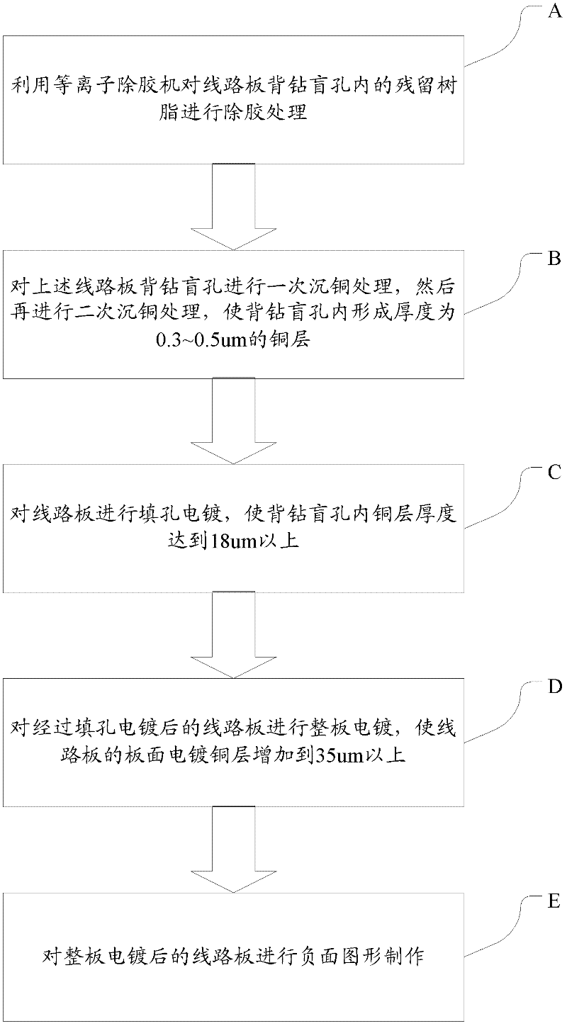
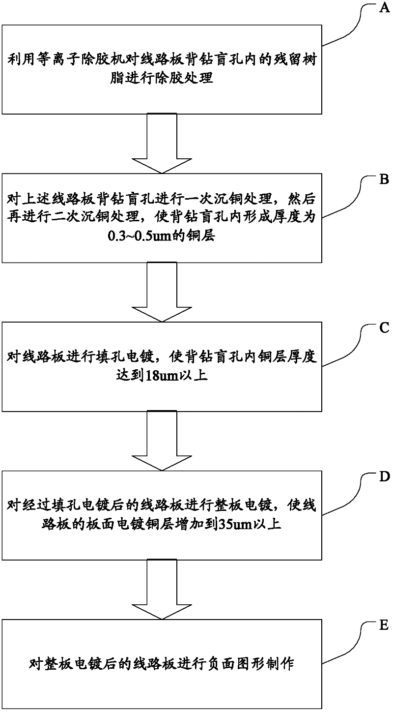
[0027] The invention provides a circuit board back-drilled blind hole electroplating process, which is mainly used to solve the problem of poor resin removal effect in blind holes and copper thickness in holes caused by chemical deglue in the current circuit board back-drilled blind hole electroplating process. Thin, after electroplating, it is easy to form defects such as voids in the hole, broken copper or open circuits, and the thickness of the copper layer in the blind hole cannot meet the requirements of 18UM in the end.

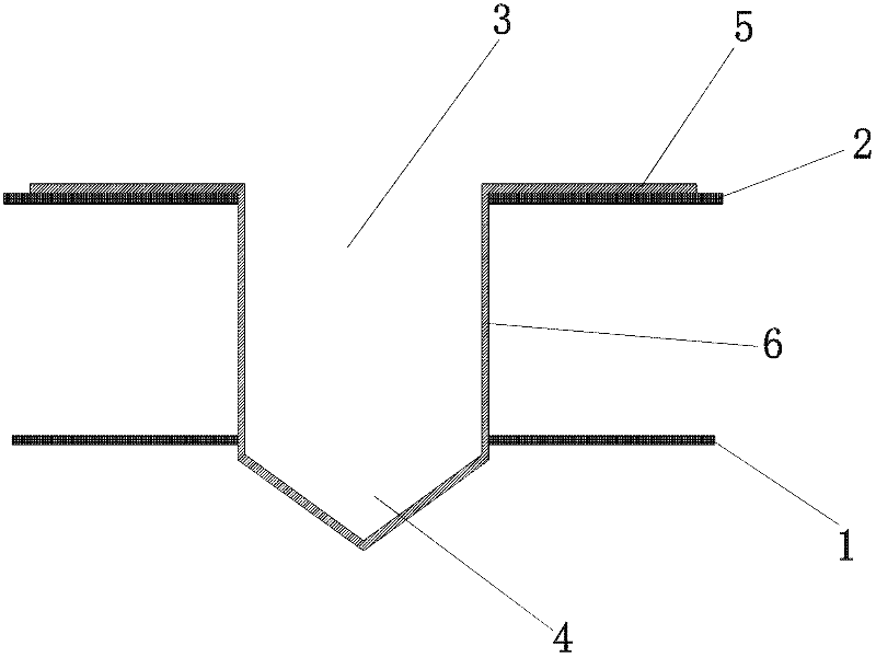
[0028] See figure 1 , figure 2 as shown, figure 1 Schematic diagram of the slicing structure for back-drilling blind holes on the circuit board; figure 2 It is a flow chart of the electroplating manufacturing process for back-drilling blind holes ...


PUM


Abstract

The invention discloses an electroplating manufacturing process, comprising the following steps of: A, utilizing a plasma degumming machine to carry out degumming treatment on residual resin in a back-drilled blind hole of a circuit board; B, carrying out primary copper deposition treatment on the back-drilled blind hole of the circuit board and then carrying out secondary copper deposition treatment to form a copper layer with the thickness of 0.3-0.5 microns in the back-drilled blind hole; and C, carrying out hole-filling electroplating on the circuit board to lead the thickness of the copper layer in the back-drilled blind hole to be more than 18 microns. According to the invention, by utilizing a plasma degumming way to treat the residual resin in the back-drilled blind hole of the circuit board, the problem that a chemical degumming speed is lower is solved, and the plasma degumming way has a good degumming effect and no residues; two times of copper deposition solve the problems that the thickness of deposited copper generated by the primary copper deposition is thin, and hollow copper depositing layers, broken copper or an open circuit is easy to generate in a process of storing or electrically pre-treating a board; and the thickness of the copper layer in the blind hole can reach to be more than 18 microns through the hole-filling electroplating, so that the thickness requirement of the back-drilled blind hole is met. Compared with the prior art, the electroplating manufacturing process provided by the invention effectively overcomes the quality defects that: the back-drilled blind hole cannot be completely degummed, the binding force is poor, and the copper in the hole is thinner and the like.

Description

Technical field: [0001] The invention belongs to the technical field of PCB production, and in particular relates to an electroplating production process for back-drilling blind holes on a circuit board. Background technique: [0002] With the continuous promotion of the information industry, the speed of digital signal transmission is getting faster and higher, the frequency is getting higher and higher, and the use of high-power amplifiers, the traditionally designed PCB board can no longer meet the needs of this high-frequency circuit. The current research on the transmission of signal integrity has proved that the useless copper part of the PTH hole has a major impact, so the use of back-drilling technology to remove this part of the hole can meet high-frequency and high-speed performance at low cost. [0003] The use of back-drilled blind holes in the PCB manufacturing process can effectively meet the needs of high-frequency circuits. The back-drilled blind holes are co...

Claims


Application Information

Patent Timeline
Patent Type & Authority Applications(China)
IPC IPC(8): H05K3/42
Inventor 宋秀金彭涛常文智陈洪胜田维丰刘晨
Owner SHENZHEN SUNTAK MULTILAYER PCB
Why Eureka
Try Eureka