A processing method for copper-plating hole filling in core board layer through-holes

A hole processing method and core layer technology are applied in the direction of printed circuits, electrical components, and the formation of electrical connections of printed components. The effects of immersion in the liquid medicine, ensuring the filling degree and ensuring the stability

Active Publication Date: 2021-04-06
清河电子科技(山东)有限责任公司
View PDF6 Cites 0 Cited by
  • Summary
  • Abstract
  • Description
  • Claims
  • Application Information

AI Technical Summary

Problems solved by technology

[0003] In the hole filling process, due to unclean foreign matter treatment, unreal and uneven copper plating filling in the through hole, the resistance caused by the virtual connection at the bottom of the laser hole increases, and the heat causes the bottom of the laser hole to break, resulting in circuit failure during use. Happening

Method used


Image

  • A processing method for copper-plating hole filling in core board layer through-holes
  • A processing method for copper-plating hole filling in core board layer through-holes
  • A processing method for copper-plating hole filling in core board layer through-holes

Examples


Embodiment 1

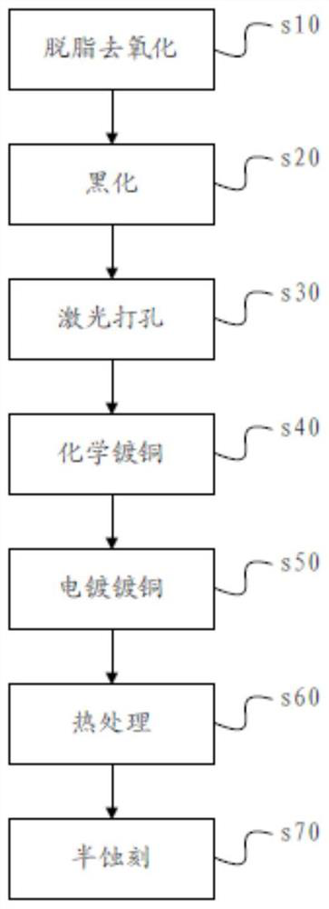
[0051] Such as figure 1 Shown is the process flow of an embodiment of the method for processing through-hole copper plating on the core board layer of the present application, including the following steps:

[0052] s10, degreasing and deoxidizing, the substrate of the core board is subjected to alkaline degreasing treatment and then put into pickling solution for weak etching treatment;

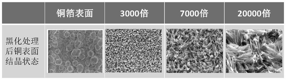
[0053] s20, blackening, the substrate after the weak etching treatment is put into a blackening agent for blackening treatment, so that the substrate forms a needle crystal surface;

[0054] s30. Laser drilling, using laser drilling equipment to perform several times of laser drilling on the front and back sides of the blackened substrate to form through holes, each time the depth of the laser drilling is 1 / 2 to 3 of the thickness of the substrate / 5;

[0055] s40. Electroless copper plating, after desmearing the punched substrate, performing electroless copper plating to deposit a uniform...

Embodiment 2

[0092] On the basis of Embodiment 1, adopt proprietary laser drilling equipment to implement step s30 laser drilling in this embodiment; as Figure 7 and Figure 8 As shown, the laser drilling equipment is provided with a workbench 100; the middle part of the workbench 100 is provided with a processing opening 110; the upper surface of the workbench 100 is provided with a pair of A clamping block 120 for clamping the substrate; a laser generator 200 is provided above and below the processing port 110;

[0093] A pair of clamping grooves 121 for clamping the substrate are provided on opposite surfaces of a pair of clamping blocks 120; the clamping grooves 121 are used to clamp the substrate that needs to be punched in this application; both sides of the substrate are inserted into the clamping The upper surface of the workbench 100 is respectively provided with an upper processing receiving mechanism 300 and a The lower processing undertaking mechanism 400;

[0094] A pair o...


PUM


Abstract

The present application provides a core plate through-hole copper-plated hole-filling processing method with excellent performance, which can eliminate the virtual connection of the through-hole copper-plated hole of the core plate. It includes the following steps: degreasing and deoxidizing, blackening, laser drilling, electroless copper plating, electroplating copper plating, heat treatment, and half etching. Among them, laser drilling adopts double-sided drilling, and electroplating copper plating includes two stages of copper plating; since the above technical scheme is adopted in this application, blackening, double-sided alternate drilling, electroless copper plating and two-stage electroplating copper plating, The processes of heat treatment and semi-etching are interlocking, adopting the idea of ​​interference copper plating, from the forming of the through hole of the core board to the step-by-step forming of the copper plating, and the tight treatment of the copper plating in the through hole. Form dense copper-plated through-holes with excellent electrical connection performance.

Description

technical field [0001] The present application relates to the technical field of PCB board production, in particular to a method for processing through-holes of a core board layer to be plated and filled with copper. Background technique [0002] With the development of electronic products such as mobile devices in the direction of lightness, thinness, shortness and smallness, the built-in printed circuit boards must also develop in the direction of light weight, small size and high circuit density. High-density interconnected printed circuit boards (HD boards) and HD board designs have emerged. The through holes in the core layer (core board layer) are used for conduction between the upper and lower sides of the circuit. At present, the general core board through hole process It is realized by the steps of blackening-laser drilling-removing foreign matter-copper plating, but the core board produced by the existing process often has the following problems: [0003] In the h...

Claims


Application Information

Patent Timeline
Patent Type & Authority Patents(China)
IPC IPC(8): H05K3/00H05K3/42
CPCH05K3/0026H05K3/423H05K2203/072H05K2203/0723H05K2203/107
Inventor 盛利召郭晓玉
Owner 清河电子科技(山东)有限责任公司
Why Eureka
Try Eureka