
Storage device and writing control method

A writing control and storage device technology, applied in information storage, static memory, digital memory information, etc., can solve the problems of reducing power consumption and increasing capacity of MRAM, achieving high-speed writing and preventing damage

Inactive Publication Date: 2012-07-04
SONY CORP
View PDF3 Cites 0 Cited by
  • Summary
  • Abstract
  • Description
  • Claims
  • Application Information

AI Technical Summary

Problems solved by technology

[0007] However, MRAM has the problem of reducing power consumption and increasing capacity

Method used


Image

  • Storage device and writing control method
  • Storage device and writing control method
  • Storage device and writing control method

Examples


Embodiment Construction

[0048] Embodiments of the present invention will be described below. Here, description will be described in the following order.

[0049]

[0050] [1-1. Overall configuration of memory block]

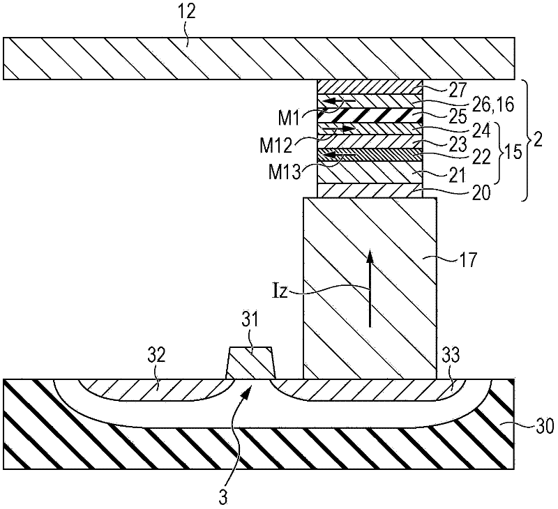
[0051] [1-2. Structure of storage unit]

[0052] [1-3. Writing and reading operations]

[0053]

[0054]

[0055] [3-1. Writing Control Unit of Embodiment]

[0056] [3-2. Comparison with the configuration generally considered from the configuration of the prior art]

[0057]

[0058]

[0059] [1-1. Overall configuration of memory block]

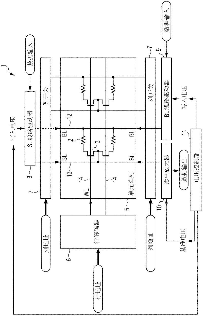
[0060] figure 1 is a diagram showing an example of the internal configuration of the memory block 1 provided in the memory device according to the embodiment of the present invention.

[0061] In the memory block 1 , memory elements 2 that store information are arranged in an array and constitute a cell array 5 . Each memory element 2 is connected to a pair of a bit line 12 (BL) and a source line 13 (SL) extending up and down on the cell...


PUM


Abstract

The invention discloses a storage device and a writing control method. The storage device is provided with a plurality of pairs of memory blocks, which have a storage layer which stores information and is configured to have a plurality of storage elements which store the information in the storage layer by the orientation of the magnetization of the storage layer being changed in accordance with the application of a writing voltage and so that selective application of the writing voltage is possible in accordance with input information to one storage element, and writing control sections, which store information which is to be written into each of the storage elements in a shift register, output one piece of information from the shift register, determine whether or not writing of the output information succeeds, and when writing has failed, the same information is output again, and when writing is successful, the next piece of information is output from the shift register.

Description

technical field [0001] The present invention relates to memory devices that perform information storage in memory elements using spin-torque magnetization reversal. Background technique [0002] With the dynamic and rapid development of various information devices ranging from mobile terminals to large-capacity servers, components such as memory and logic constituting information devices are required to have further higher performance, such as high integration, high speed, low power consumption, etc. . [0003] Specifically, the progress of semiconductor non-volatile memory is remarkable, and the widespread use of flash memory as large-capacity file storage is on the rise along with the momentum driven by hard disk drives. [0004] On the other hand, the development of code storage and working memory is attracting attention, and the development of semiconductor nonvolatile memory is also being continuously carried out to replace NOR flash memory, DRAM, etc. which are genera...

Claims


Application Information

Patent Timeline
Patent Type & Authority Applications(China)
IPC IPC(8): G11C11/16
CPCH01L43/08G11C11/1675G11C7/06G11C11/16H01L27/105G11C19/00G11C11/1677H01L29/82G11C11/15G11C11/161
Inventor 肥后丰细见政功大森广之别所和宏山根一阳内田裕行浅山徹哉
Owner SONY CORP
Learn More