
Manufacturing method of package substrate

A technology for packaging substrates and processing methods, which is applied in metal material coating technology, gaseous chemical plating, coating, etc., can solve problems such as reducing line density, noise interference, and occupying substrate wiring space, so as to reduce processing costs and reduce Effect of noise interference and expansion of effective wiring space

Active Publication Date: 2012-07-04
SHENNAN CIRCUITS
View PDF4 Cites 4 Cited by
  • Summary
  • Abstract
  • Description
  • Claims
  • Application Information

AI Technical Summary

Problems solved by technology

These electroplated leads occupy the wiring space of the substrate, relatively reduce the density of the circuit, and are easy to cause noise interference when constructing high-frequency chips

Method used


Image

  • Manufacturing method of package substrate
  • Manufacturing method of package substrate
  • Manufacturing method of package substrate

Examples


Embodiment Construction

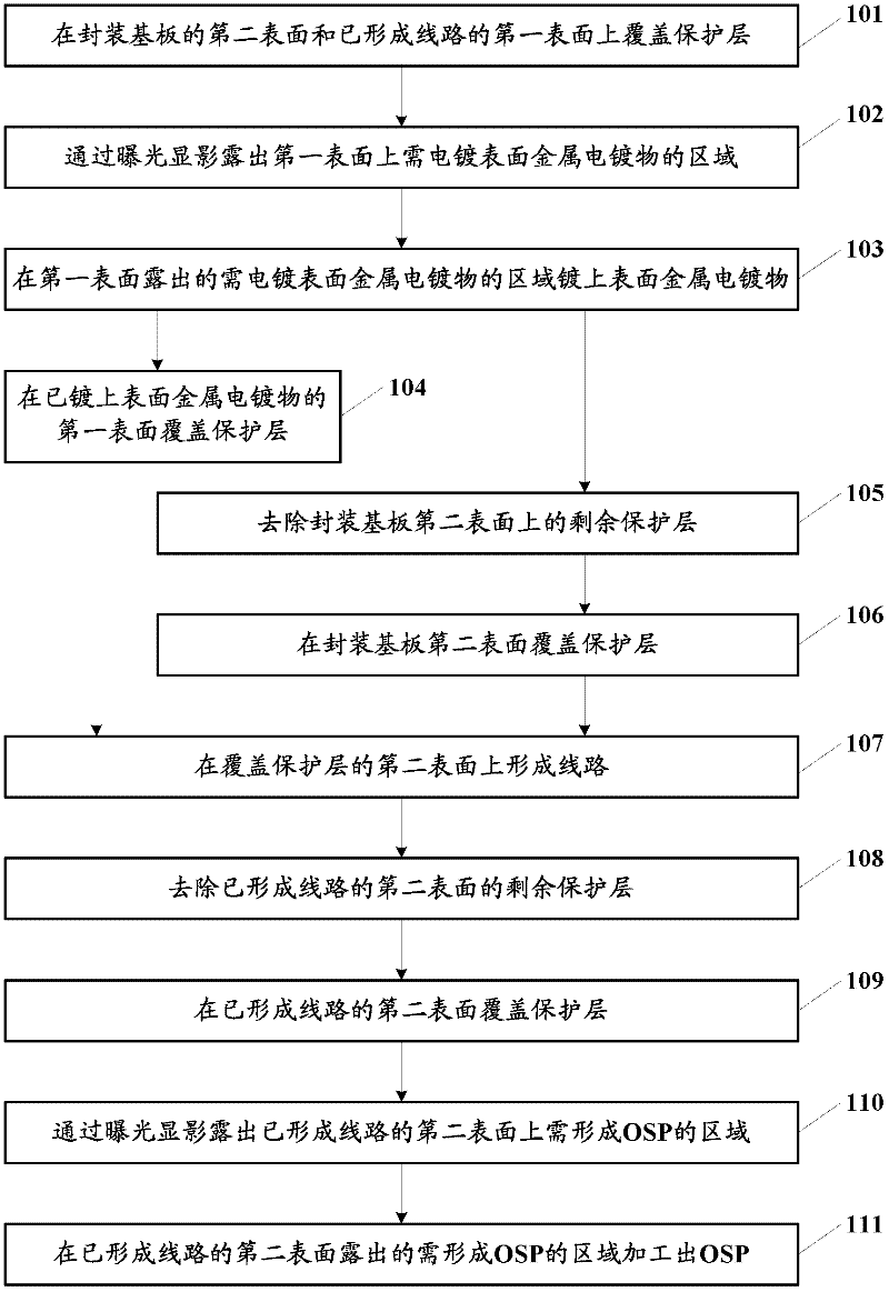
[0039] The embodiment of the present invention provides a packaging substrate processing method in order to avoid or minimize the use of electroplating leads in the process of electroplating nickel and gold on the substrate.

[0040] The following will clearly and completely describe the technical solutions in the embodiments of the present invention with reference to the accompanying drawings in the embodiments of the present invention. Obviously, the described embodiments are only some, not all, embodiments of the present invention. Based on the embodiments of the present invention, all other embodiments obtained by persons of ordinary skill in the art without creative work belong to the protection scope of the present invention

[0041] Each will be described in detail below.

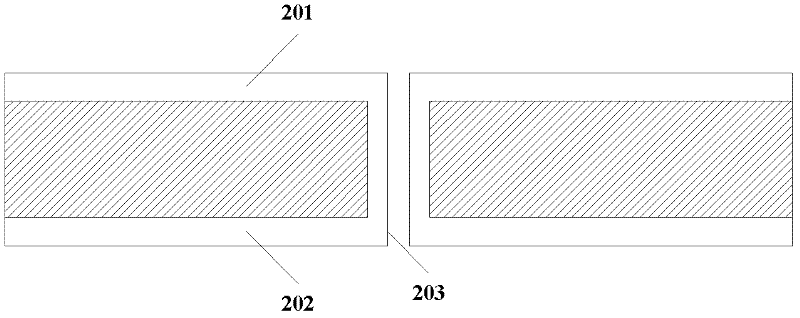
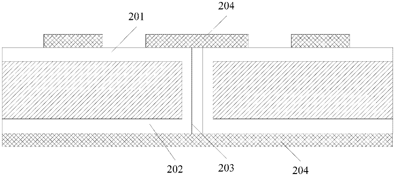
[0042] An embodiment of the packaging substrate processing method of the present invention may include:

[0043] A protective layer is covered on the second surface of the packaging substrate and th...


PUM


Abstract

The embodiment of the invention discloses a manufacturing method of a package substrate, which comprises steps of respectively covering a protection layer on a second surface and a first surface of the package substrate, wherein a circuit is formed on the first surface, and providing at least one via hole between the first surface and the second surface of the package substrate; exposing an area needed to be electroplated with a surface metal electroplate by exposure development on the first surface; electroplating the area needed to be electroplated with the surface metal electroplate on the first surface; covering another protection layer on the firs surface; removing the residual protection layer on the second surface; covering another protection layer on the second surface; forming another circuit on the second surface; removing the another residual protection layer on the second surface where the circuit is formed; covering a protection layer on the second surface and exposing an area where an OSP (organic solderability preservative) is needed to form on, wherein the area is on the second surface; and manufacturing the OPS on the area where an OSP is needed to form, wherein the area is on the second surface. The method of the embodiment of the invention is helpful for avoiding or reducing electroplated lead usage in the substrate electroplating process as much as possible.

Description

technical field [0001] The invention relates to the technical field of circuit board processing, in particular to a packaging substrate processing method. Background technique [0002] In the packaging industry, the production of the chip itself is generally called zero-level packaging, and the packaging of the chip on the packaging substrate (or substrate, carrier) is called the first-level packaging. It is called secondary packaging. [0003] The electrical conduction between the substrate and the chip in the first-level packaging is usually realized by wire bonding. The conduction of the electrical properties of the chip and the substrate; the coating method of wire bonding on the surface of the substrate (or I / O contact) during processing is electroplated nickel gold, and nickel gold is plated on these electrical contact pads to ensure The stability of the electrical connection with the chip; the electrical conduction between the other side of the substrate and the pri...

Claims


Application Information

Patent Timeline
IPC IPC(8): H01L21/60C23C16/06
Inventor 范铮刘良军杨智勤
Owner SHENNAN CIRCUITS
Learn More