

Light-emitting device and producing method thereof
A technology for a light-emitting device and a manufacturing method, which is applied to electrical components, circuits, semiconductor devices, etc., can solve the problems of lead shielding light, lead disconnection, time required for assembling leads, etc. The effect of taking out efficiency
- Summary
- Abstract
- Description
- Claims
- Application Information
AI Technical Summary
Problems solved by technology
Method used
Image

Examples
Embodiment 1
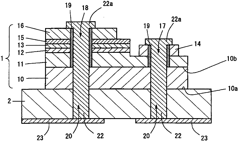
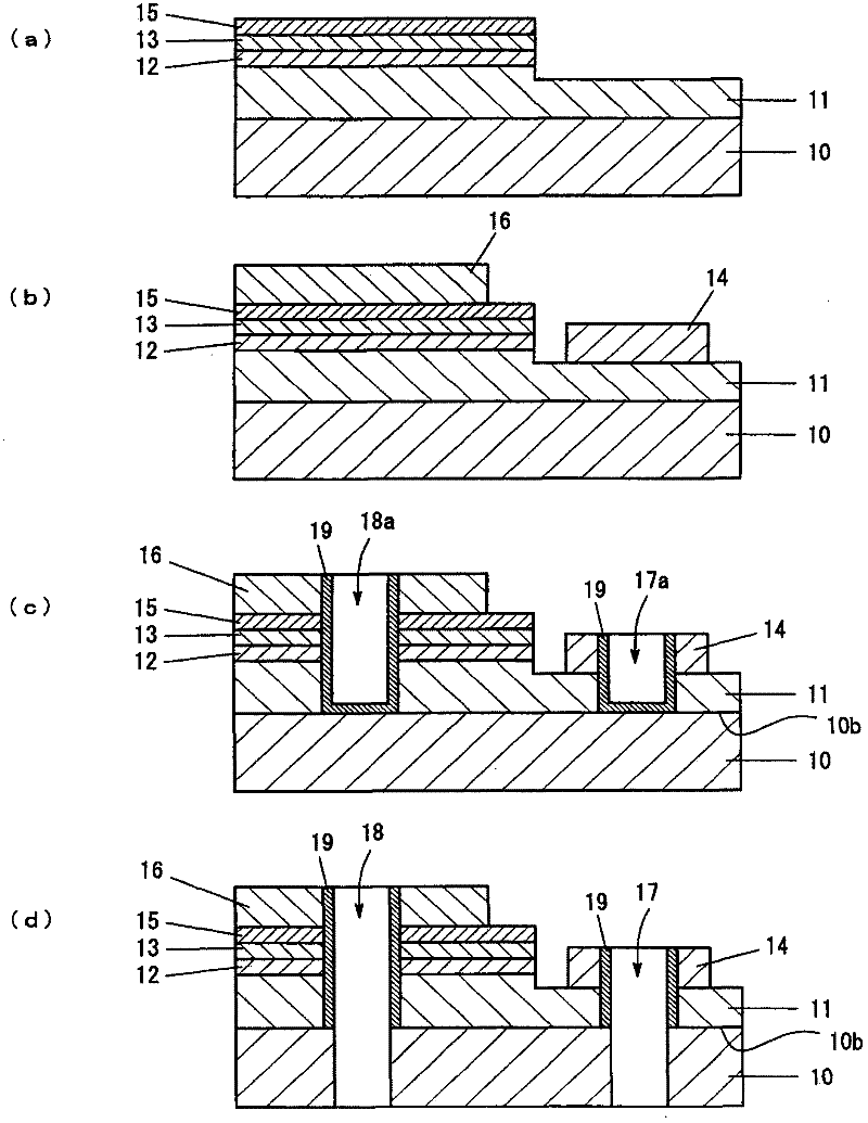
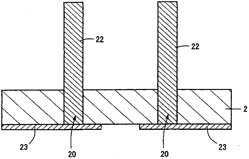
[0031] figure 1 It is a figure showing the structure of the light-emitting device of Example 1. The light emitting device is constituted by: a face-up type light emitting element 1 composed of a Group III nitride semiconductor; and a submount 2 composed of AlN.
[0032] The light-emitting element 1 has a sapphire substrate 10 on which an n-type layer 11 made of a Group III nitride semiconductor, a light-emitting layer 12 , and a p-type layer 13 are formed in this order. The structures of the n-type layer 11, the light-emitting layer 12, and the p-type layer 13 may be any structures known in the art as structures of light-emitting elements. The n-type layer 11 is, for example, a structure in which an n-type contact layer made of GaN and embedded with Si at a high concentration and an n cladding layer made of GaN are laminated in this order from the sapphire substrate 10 side. The light emitting layer 12 has, for example, an MQW structure in which a barrier layer made of GaN a...
Embodiment 2
[0048] Figure 5 It is a figure showing the structure of the light-emitting device of Example 2. The light emitting device of Example 2 is a light emitting device in which two light emitting elements 1a, 1b are mounted on a submount 200, and these two light emitting elements 1a, 1b are connected in series. The structures of the light emitting elements 1a and 1b are the same as those of the light emitting element 1 of the first embodiment.
[0049] Install abutments 200 times Figure 5 As shown, four through-holes 201a-d are provided, and rod-shaped electrodes 202a-d are respectively inserted into the through-holes 201a-d so as to be supported and erected. The rod-shaped electrodes 202a, b are arranged in the mounting area of the light-emitting element 1a and at positions opposite to the p-pad electrode 16 and the n-pad electrode 14 of the light-emitting element 1a (in a plan view, the p-pad electrode 16 and the n-pad electrode 14), the rod-shaped electrodes 202c and d are...
Embodiment 3
[0054] Figure 6 It is a figure showing the structure of the light-emitting device of Example 3. The light-emitting device of Example 3 is composed of a light-emitting element 300 with a vertical structure and a submount 400 .
[0055] The light-emitting element 300 has a GaN substrate 301 on which an n-type layer 302 made of a Group III nitride semiconductor, a light-emitting layer 303 , and a p-type layer 304 are stacked in this order. An ITO electrode 305 is formed on the p-type layer 304 , and a p pad electrode 306 is formed on the ITO electrode 305 .
[0056] The light emitting element 300 is provided with a through hole 307, which penetrates in a direction perpendicular to the element surface from the surface of the p pad electrode 306 to the back surface 301a of the GaN substrate 301 (the surface opposite to the side where the n-type layer 302 is formed). . An insulating film 308 is formed on the side surface of the through hole 307 to prevent current leakage and sho...
PUM
 Abstract
Description
Claims
Application Information