
Stacked-assembled substrate and stacked assembly method of TSOP (Thin Small Outline Package) integrated circuits

A technology of integrated circuits and printed circuit boards, which is applied in the field of stacking boards for TSOP integrated circuits, can solve the problems of increased integrated circuit prices, inability to use equipment, and low product yield, so as to control costs, realize quantitative production, and improve The effect of capacity

Active Publication Date: 2012-07-04
SUZHOU ETRON TECH CO LTD
View PDF4 Cites 1 Cited by
  • Summary
  • Abstract
  • Description
  • Claims
  • Application Information

AI Technical Summary

Problems solved by technology

With the continuous expansion and improvement of the application range and application level of computer networks, higher requirements are constantly put forward for the storage capacity, read and write speed and error correction tolerance of computer data information. The capacity is getting bigger and bigger, but the price of the integrated circuit is also increasing
In addition, the existing integrated circuit stacking and assembly method usually directly solders two chips by hand, which not only cannot be quantitatively produced by equipment, but also has low production capacity, and there are problems such as low product yield and inability to repair

Method used

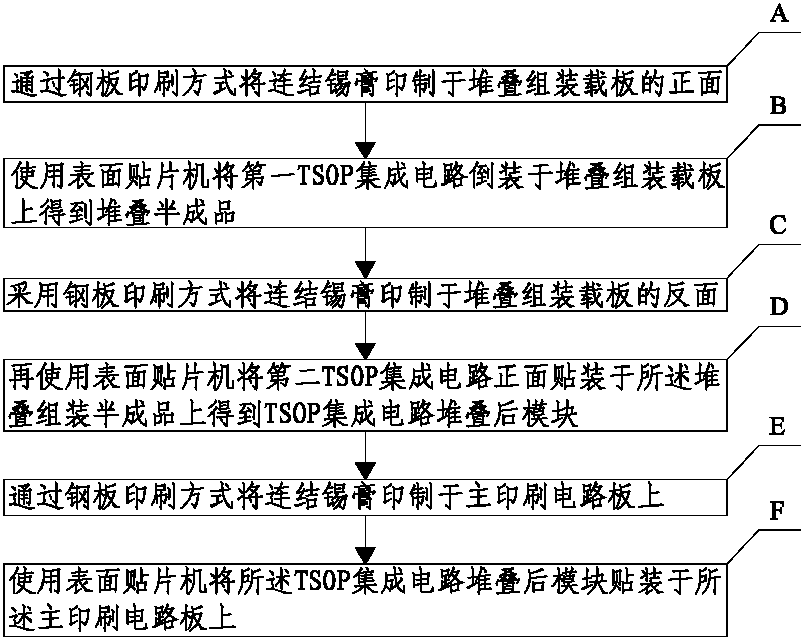
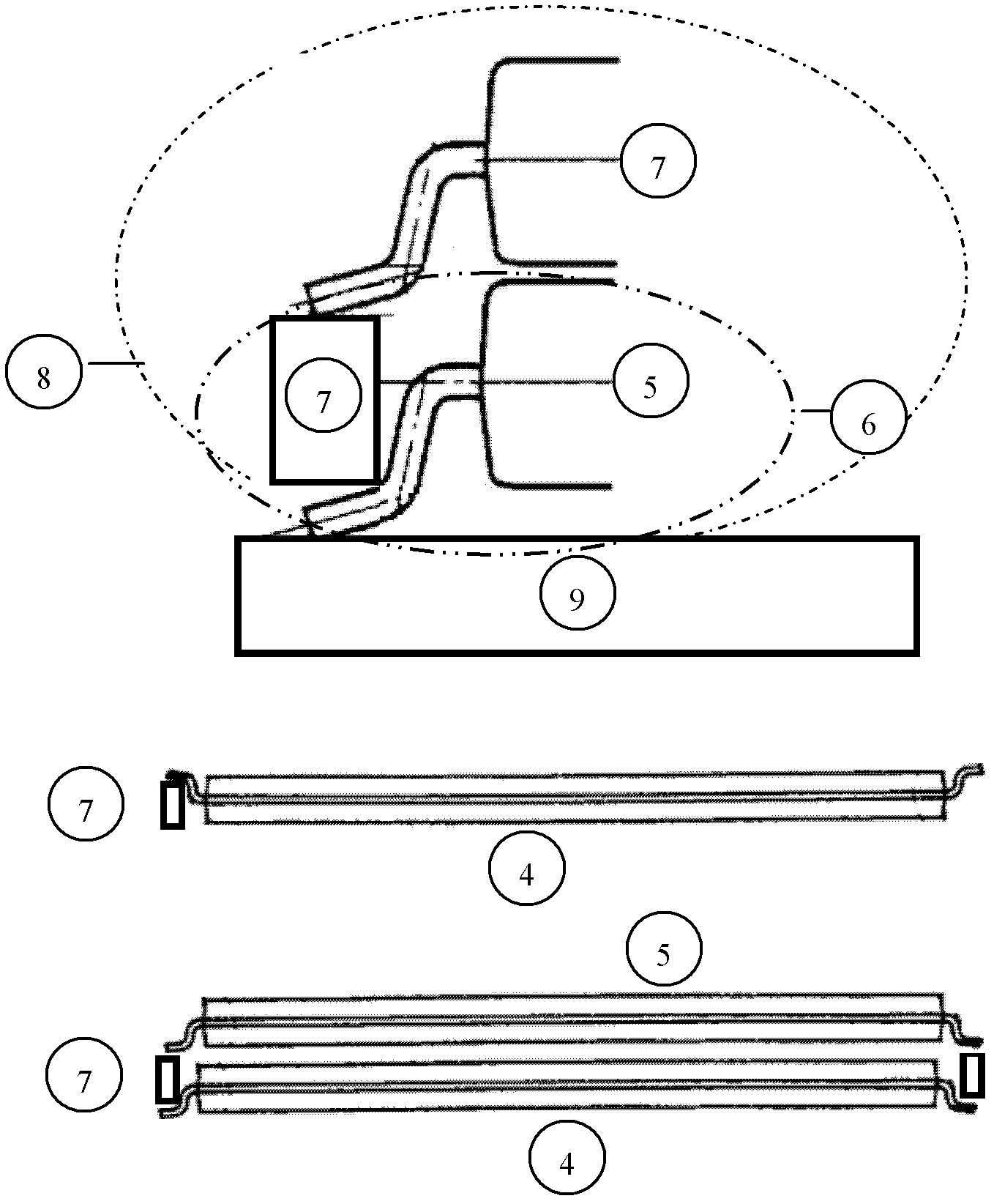

Image

  • Stacked-assembled substrate and stacked assembly method of TSOP (Thin Small Outline Package) integrated circuits
  • Stacked-assembled substrate and stacked assembly method of TSOP (Thin Small Outline Package) integrated circuits
  • Stacked-assembled substrate and stacked assembly method of TSOP (Thin Small Outline Package) integrated circuits

Examples


Embodiment Construction

[0025] The specific implementation manners of the present invention will be further described in detail below in conjunction with the accompanying drawings and embodiments. The following examples are used to illustrate the present invention, but are not intended to limit the scope of the present invention.

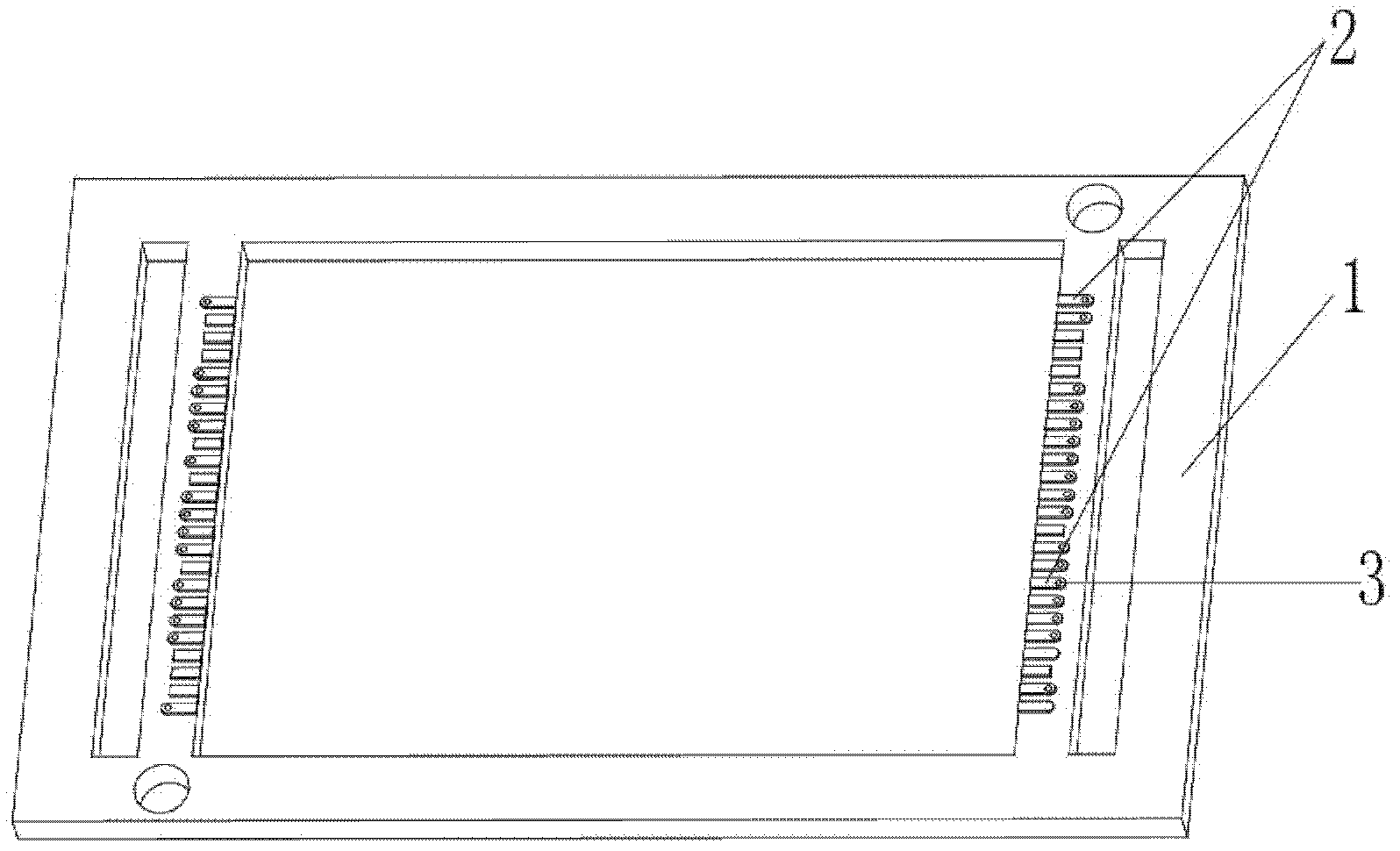
[0026] Such as figure 1 As shown, the stacked group loading board of the TSOP integrated circuit of the present invention includes a printed circuit board 1, and the front and back sides of the printed circuit board 1 are provided with TSOP welding pads 2, and the TSOP welding pads 2 are provided with There are through holes 3 for electrically connecting two TSOP integrated circuits mounted on the front and back sides of the printed circuit board 1 through the TSOP welding pads 2 . The number of the printed circuit board 1 can be single or multiple. The size of the stacking board is adapted to the shoulder width of the soldering pins of the TSOP integrated circuit.

[0...


PUM


Abstract

The invention discloses a stacked-assembled substrate and a stacked assembly method of TSOP (Thin Small Outline Package) integrated circuits. The stacked-assembled substrate comprises a printed circuit board, wherein the front and the back of the printed circuit board are provided with TSOP welded pads. Through holes are arranged on the TSOP welded pads and are used for electrically connecting two TSOP integrated circuits stuck on the front and the back of the printed circuit board through the TSOP welded pads. The TSOP integrated circuits are stacked and assembled through the stacked-assembled substrate, so that the quantitative production of the TSOP integrated circuits can be realized, the capacity is increased, and the cost of products is reduced. According to the stacked-assembled substrate, the product yield of assembly production can be increased, and after-sales services are convenient. In addition, the method uses the existing equipment and does not need replace special or higher-end equipment to support output, and therefore the cost is further controlled.

Description

technical field [0001] The invention relates to the technical field of integrated circuit assembly, in particular to a stacking group loading board of a TSOP integrated circuit and a stacking assembly method. Background technique [0002] In recent years, the application of computer network has expanded and penetrated into various fields of economy, politics and social life. With the continuous expansion and improvement of the application range and application level of computer networks, higher requirements are constantly put forward for the storage capacity, read and write speed and error correction tolerance of computer data information. The capacity is getting larger and larger, but the price of the integrated circuit is also increasing. In addition, the existing integrated circuit stacking and assembly method usually directly solders two chips by hand, which not only cannot use equipment for quantitative production, but also has low production capacity, and there are pr...

Claims


Application Information

Patent Timeline
IPC IPC(8): H05K1/18H05K1/11H05K3/34
Inventor 钱新栋陈献祥
Owner SUZHOU ETRON TECH CO LTD
Learn More