Array substrate, manufacturing method thereof, and liquid crystal display device
A technology for liquid crystal display devices and array substrates, which is applied in semiconductor/solid-state device manufacturing, instruments, semiconductor devices, etc., can solve problems such as insufficient, and achieve the effect of improving utilization rate and saving area
- Summary
- Abstract
- Description
- Claims
- Application Information
AI Technical Summary
Problems solved by technology
Method used
Image

Examples
no. 1 example
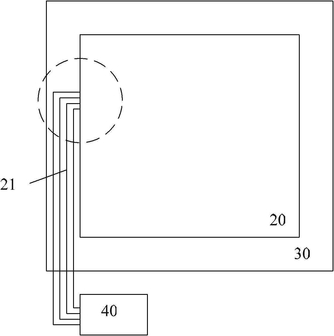
[0051] refer to Figure 4 , is a schematic top view structure diagram of the array substrate according to the first embodiment of the present invention.
[0052] The array substrate is divided into a display area and a frame area surrounding the display area. To simplify the illustration, Figure 4 Only a schematic top view of a part of the display area is shown in . The display area includes: a glass substrate (not shown in the figure); a plurality of scanning lines on the glass substrate: scanning line 101, scanning line 103, scanning line 105, etc.; a plurality of data lines: data line 102, data Line 104, data line 106, etc., each scan line is orthogonal to the data line and is insulated from each other. The data line and the scan line are made of different layers of metal and are separated by an insulating medium layer. The data line is located above the scan line, and the two will display The area is divided into a plurality of pixel areas arranged in an array, and each...
no. 2 example
[0087] In the above embodiments, the scan connection lines are directly connected to the scan lines through via holes in the display area, which is easily limited by wiring during actual manufacturing. As another optional embodiment, the scanning connection line and the scanning line may also be indirectly connected through a via hole located thereon and other layer metals located in the via hole.
[0088] Specifically, refer to Figure 18 As shown in FIG. 2 , it is a schematic top view structure diagram of the array substrate according to the second embodiment of the present invention. Will Figure 18 and Figure 4 It can be seen from the comparison that the difference between this embodiment and the first embodiment is only that the connection structure between the scanning connection lines and the scanning lines is indirectly connected through other metal layers.
[0089] For a better description of the above connection structure, please refer to Figure 19 ,for Figur...
no. 3 example
[0098] In the above embodiments, the scanning connection lines are located between the first pixel electrode and the second pixel electrode, that is, at the center of the pixel area. As another optional embodiment, the scanning connection lines can also be located in a part of the pixel area. side, and adjacent to the data line of the adjacent pixel area.
[0099] Figure 24 It is a schematic top view structure diagram of the array substrate according to the third embodiment of the present invention. to combine Figure 24 and Figure 4 As shown, the only difference between this embodiment and the first embodiment is that the scanning connection line is located between the pixel electrode and the data line in the adjacent pixel area. Specifically, the scanning connection line 202 is located between the first pixel electrode 1201 and the data line 104, and is located below the second transparent electrode 130 and parallel to the data line 104; the scanning connection line 203...
PUM
 Abstract
Description
Claims
Application Information
 - R&D
- Intellectual Property
- Life Sciences
- Materials
- Tech Scout
- Unparalleled Data Quality
- Higher Quality Content
- 60% Fewer Hallucinations
Browse by: Latest US Patents, China's latest patents, Technical Efficacy Thesaurus, Application Domain, Technology Topic, Popular Technical Reports.
© 2025 PatSnap. All rights reserved.Legal|Privacy policy|Modern Slavery Act Transparency Statement|Sitemap|About US| Contact US: help@patsnap.com