Low-temperature polysilicon display device and manufacturing method thereof

A technology of low-temperature polysilicon and liquid crystal display devices, applied in semiconductor/solid-state device manufacturing, optics, instruments, etc., can solve problems such as long time, impact on production capacity, and high cost, and achieve the effects of increasing production capacity, reducing use, and reducing time

Active Publication Date: 2012-07-11
TCL CHINA STAR OPTOELECTRONICS TECH CO LTD
View PDF4 Cites 30 Cited by
  • Summary
  • Abstract
  • Description
  • Claims
  • Application Information

AI Technical Summary

Problems solved by technology

Such a process is costly and takes a long time to complete a process, seriously affecting production capacity

Method used


Image

  • Low-temperature polysilicon display device and manufacturing method thereof
  • Low-temperature polysilicon display device and manufacturing method thereof
  • Low-temperature polysilicon display device and manufacturing method thereof

Examples


Embodiment Construction

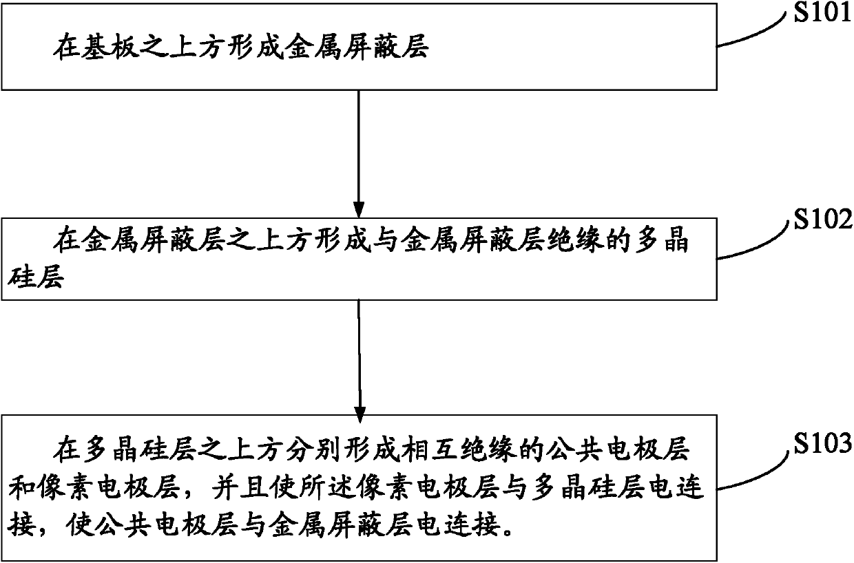
[0020] In the following, the embodiment of the low temperature polysilicon display device of the present invention will be described in detail, so as to more clearly disclose the details and spirit of the present invention.

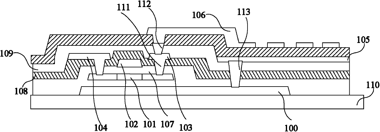
[0021] Such as figure 2 as shown, figure 2 It is a schematic partial cross-sectional view of a thin film transistor substrate in an embodiment of a low-temperature polysilicon display device of the present invention. The low-temperature polysilicon display device of the present invention includes:

[0022] The substrate 110 , the metal shielding layer 100 , the polysilicon layer 101 , the gate metal layer 102 , the source metal layer 103 , the drain metal layer 104 , the common electrode layer 105 and the pixel electrode layer 106 .

[0023] The metal shielding layer 100 is disposed on the substrate 110 to reduce leakage current caused by light.

[0024] A polysilicon layer 101 insulated from the metal shielding layer 100 is disposed on the metal shi...


PUM


Abstract

The invention discloses a low-temperature polysilicon display device and a manufacturing method thereof. The manufacturing method comprises the following steps of: forming a metal shielding layer on a substrate; forming a polysilicon layer insulated from the metal shielding layer above the metal shielding layer; and respectively forming a public electrode layer and a pixel electrode layer which are insulated from each other above the polysilicon layer, wherein the pixel electrode layer is electrically connected with the polysilicon layer, and the public electrode layer is electrically connected with the metal shielding layer. Due to the mode, a resistance value of the public electrode layer can be reduced, a delay effect caused by overlarge resistance value of the public electrode layer, the using amount of a one-time mask and the time for finishing a one-time process flow are reduced, the cost is reduced, and the yield is increased.

Description

technical field [0001] The invention relates to the field of display technology, in particular to a low-temperature polysilicon display device and a manufacturing method thereof. Background technique [0002] Low-temperature polycrystalline technology has been widely used in the field of liquid crystal displays and / or organic light-emitting diodes, and combined with in-plane switching (In-PlaneSwitching, IPS) or fringe field switching (FringeFieldSwitching, FFS) technology can achieve better display characteristics and better to meet the needs of consumers. [0003] Such as figure 1 As shown, in the prior art, a low temperature polysilicon display device includes: a substrate 10 , a metal shielding layer 11 , a polysilicon layer 12 , a common electrode 13 and a metal layer 14 . A metal shielding layer 11 , a polysilicon layer 12 , a common electrode 13 and a metal layer 14 are sequentially formed on the substrate 10 , wherein a part of the polysilicon layer 12 serves as a ...

Claims


Application Information

Patent Timeline
Patent Type & Authority Applications(China)
IPC IPC(8): H01L21/77H01L27/02H01L23/552
CPCH01L29/78633H01L2924/0002H01L21/77H01L27/124G02F1/136209H01L23/552
Inventor 周秀峰
Owner TCL CHINA STAR OPTOELECTRONICS TECH CO LTD
Why Eureka
Try Eureka