Layout and schematic diagram consistency comparison method for multi-voltage chip design

A chip design, multi-voltage technology, applied in the direction of electrical digital data processing, calculation, special data processing applications, etc., can solve the problems that LVS cannot reflect the real situation, LVS cannot reflect the situation, and the efficiency of LVS is low, so as to save physical verification The effect of shortening time, shortening time, improving efficiency and reliability

Active Publication Date: 2012-07-18
SHANGHAI HUAHONG GRACE SEMICON MFG CORP
View PDF3 Cites 17 Cited by
  • Summary
  • Abstract
  • Description
  • Claims
  • Application Information

AI Technical Summary

Problems solved by technology

[0004] The first method is to modify the runset. In the runset, multiple power pins of low-power related cells are forcibly defined as one power supply, so that LVS can succeed, but this method will bring certain risks, causing LVS to fail to reflect the real situation.
[0005] The second method is to modify and connect multiple power supplies of low-power-related cells into one power supply in the layout,

Method used


Image

  • Layout and schematic diagram consistency comparison method for multi-voltage chip design
  • Layout and schematic diagram consistency comparison method for multi-voltage chip design
  • Layout and schematic diagram consistency comparison method for multi-voltage chip design

Examples


Example Embodiment

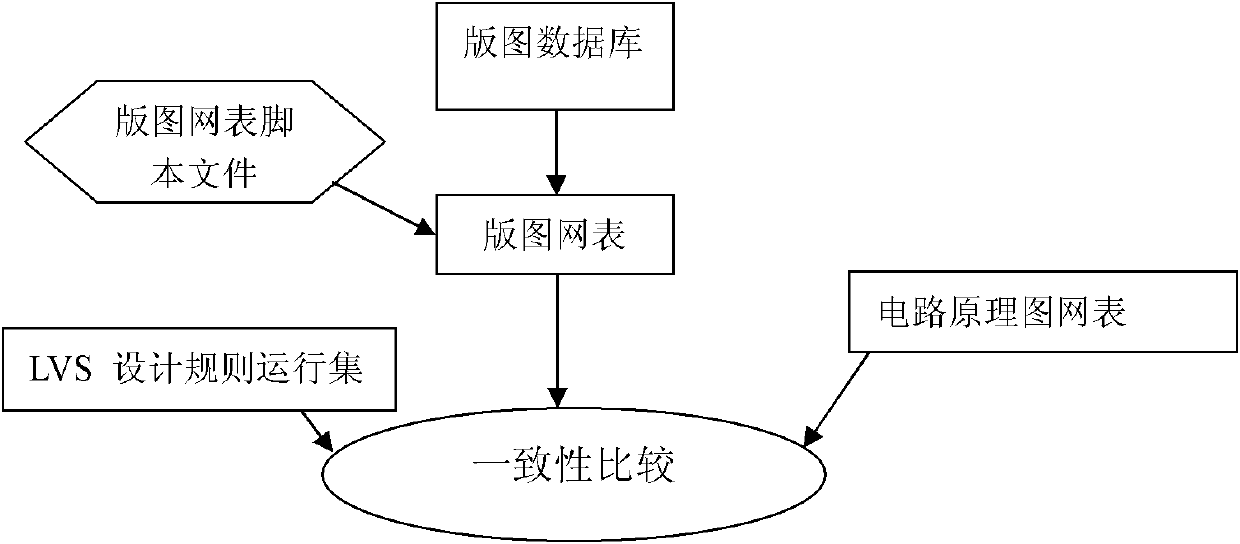
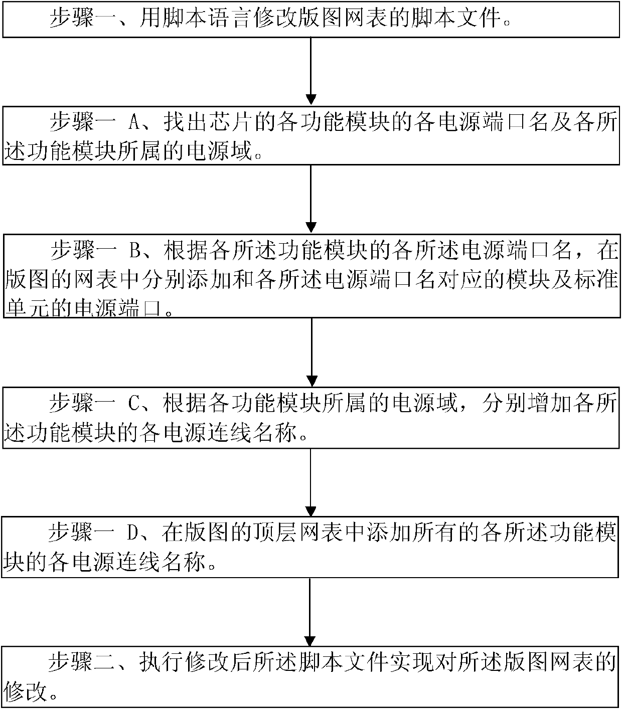
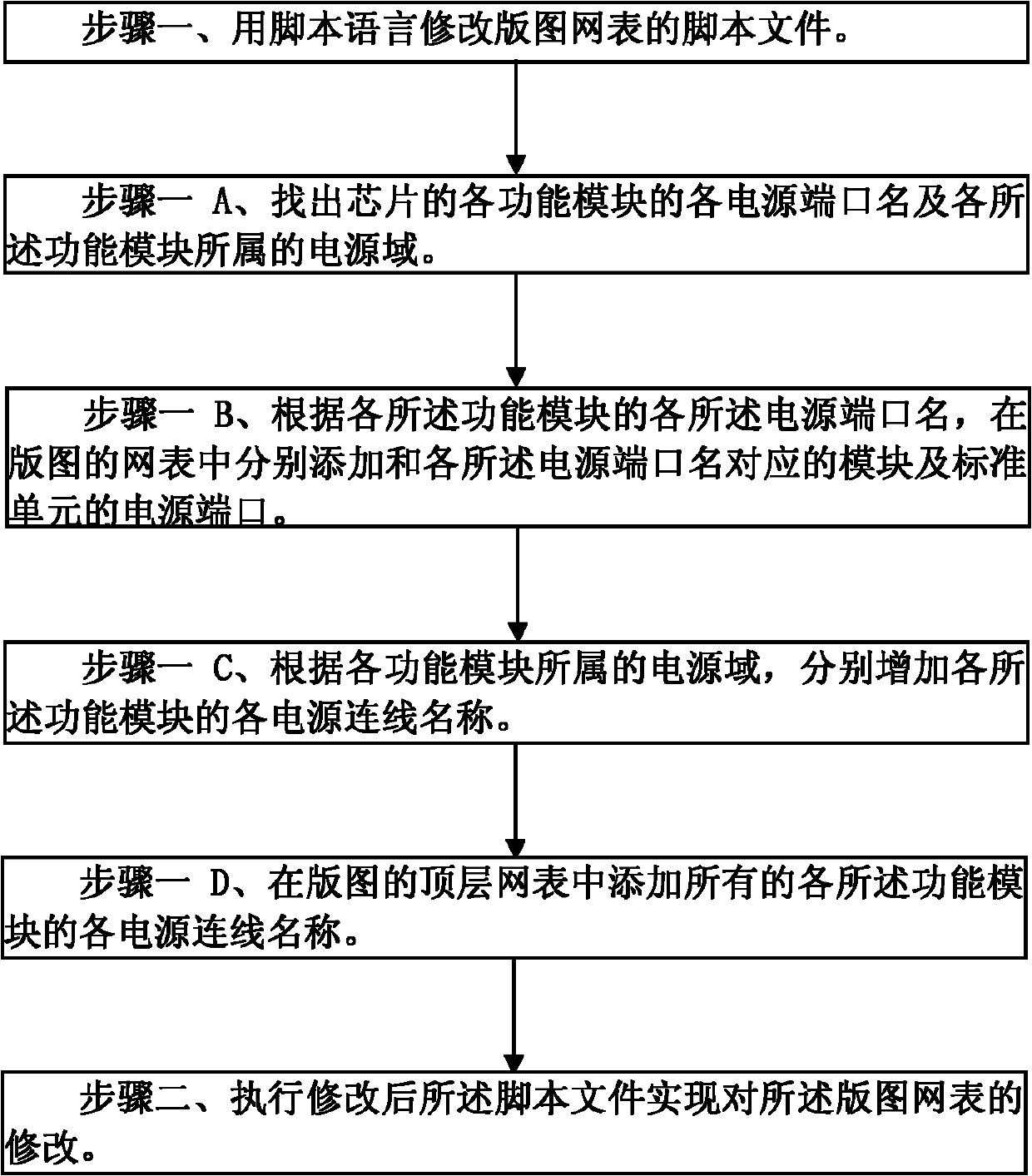
[0022] Such as figure 2 Shown is the flow chart of the method of the present invention, the layout and principle of the multi-voltage chip design of the embodiment of the present invention Figure one The consistency comparison method includes the following steps:

[0023] Step 1. Use PERL to modify the script file MPower.pl of the layout netlist. The following steps are included when modifying the MPOwer.pl:

[0024] Step 1A. Find out the name of each power port of each functional module of the chip and the power domain to which each power port belongs. Each of the functional modules includes two categories: power normally-on modules and power-off modules.

[0025] Step 1B. According to the name of each power port of each of the functional modules, respectively add the module and the power port of the standard unit corresponding to each of the power port names in the layout netlist.

[0026] Step 1C: According to the power domain to which each functional module belongs, add each po...


PUM


Abstract

The invention discloses a layout and schematic diagram consistency comparison method for multi-voltage chip design, which comprises the steps of: amending a script file of a layout netlist and executing the script file to amend the layout netlist. The procedure of amending the script file comprises the steps of: finding the power supply port titles and subject power supply domains of functional modules of a chip; respectively adding modules corresponding to the power supply port titles and power supply ports of standard units in the layout netlist; adding the power supply connecting line titles in the layout netlist according to the subject power supply domains of the functional modules; and adding the power supply connecting line titles of all functional modules in the top layer of the layout netlist. The method of the invention has the advantages of improving the check efficiency and reliability, reducing the check risk and saving the design cost.

Description

technical field [0001] The present invention relates to the field of semiconductor integrated circuit manufacturing, in particular to the layout and principle of a multi-voltage chip design Figure 1 consistency comparison method. Background technique [0002] In the existing chip design, the layout and principle must be carried out after the chip layout design is completed. Figure 1 Consistency comparison (Layout versus Schematic, LVS) to ensure the consistency of layout and circuit schematic. Such as figure 1 As shown, it is the flow chart of the existing LVS, the steps of the existing LVS include the steps of extracting the layout netlist (Layout Netlist) from the layout database (Layout Database), and performing the comparison under the environment of the LVS design rule run set (Runset) A step of performing a consistency comparison (Compare) between the layout netlist and the schematic netlist (Schematic Netlist). The layout netlist can also be modified through a la...

Claims


Application Information

Patent Timeline
IPC IPC(8): G06F17/50
Inventor 周喆
Owner SHANGHAI HUAHONG GRACE SEMICON MFG CORP
Why Eureka
Try Eureka