Micro-strip step impedance resonator and micro-strip wave filter

A technology of microstrip filter and step impedance, which is applied in the direction of resonators, waveguide devices, electrical components, etc., can solve the problems of small coupling coefficient and poor filter performance, achieve large coupling coefficient, reduce size, The effect of improving performance

Active Publication Date: 2015-02-11
INST OF PHYSICS - CHINESE ACAD OF SCI
View PDF3 Cites 0 Cited by
  • Summary
  • Abstract
  • Description
  • Claims
  • Application Information

AI Technical Summary

Problems solved by technology

[0007] The purpose of the present invention is to provide a microstrip step impedance resonator and a microstrip filter, which are used to solve the problem that the coupling coefficient between two resonators in the prior art is small, and the simultaneous existence of non-adjacent resonators is relatively serious. parasitic coupling, resulting in poor filter performance

Method used


Image

  • Micro-strip step impedance resonator and micro-strip wave filter
  • Micro-strip step impedance resonator and micro-strip wave filter
  • Micro-strip step impedance resonator and micro-strip wave filter

Examples


Embodiment 1

[0048] refer to Figure 4 , 5a , using a microstrip line to form a microstrip resonator, the microstrip line is a superconducting microstrip line, the upper layer is a microstrip conductor 3 and the lower layer ground plane conductor 1 is YBCO high temperature superconducting film or metal, and the middle 2 is a dielectric The constant is ξ r medium. The microstrip line selected in this embodiment adopts the crystal medium LaAlO 3 , whose dielectric constant ξ r =23.65, the start section of the microstrip line is adjacent to the end section of the microstrip line. t is the thickness of the upper conductor 3, W is the width of the upper conductor 3, h is the thickness of the medium, ξ r is the dielectric constant of the medium.

[0049] Figure 5aIt is a superconducting microstrip resonator pattern designed according to the frequency of 1747.5MHz in this embodiment, the pattern size is 3.42mm×3.6mm (length×width), and the line width of the microstrip line is 0.14mm and 1...

Embodiment 2

[0054] refer to Figure 4 , 5a , using a microstrip line to form a microstrip resonator, the microstrip line is a superconducting microstrip line, the upper layer is a microstrip conductor 3 and the lower layer ground plane conductor 1 is YBCO high temperature superconducting film or metal, and the middle 2 is a dielectric The constant is ξ r medium. The microstrip line selected in this embodiment adopts the crystal medium LaAlO 3 , whose dielectric constant ξ r =23.65.

[0055] Figure 5a It is a superconducting microstrip resonator pattern designed according to the frequency of 1747.5MHz in this embodiment, the pattern size is 3.42mm×3.6mm (length×width), and the line width of the microstrip line is 0.14mm and 1.16mm. In this embodiment, the initial section 51 of the microstrip line, with a line length of 3.32 mm, and the end section 52 of the microstrip line, with a line length of 3.18 mm, are arranged in the same direction and adjacent to each other.

[0056] to ref...

Embodiment 3

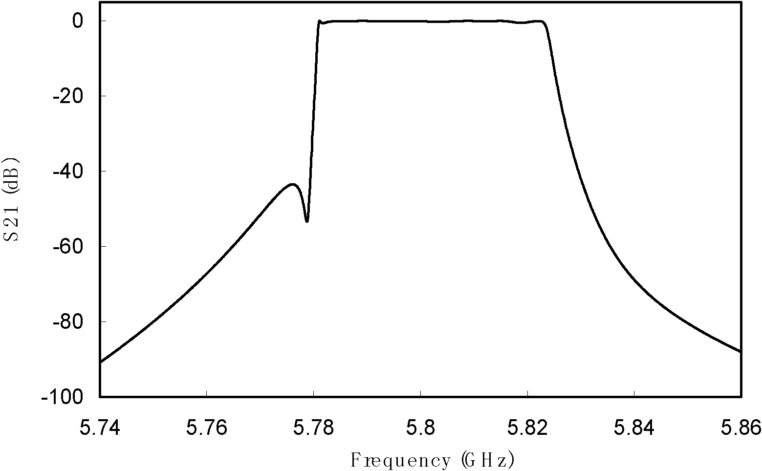
[0059] The center frequency of the filter is 1747.5MHz and the bandwidth is 75MHz. refer to Figure 4 , 5a , using a microstrip line to form a microstrip filter, the microstrip line is a superconducting microstrip line, the upper layer of the microstrip conductor 3 and the lower layer of the ground plane conductor 1 are both YBCO high-temperature superconducting films, and the middle 2 is a dielectric constant of ξ r medium. The microstrip line selected in this embodiment adopts the crystal medium LaAlO 3 , whose dielectric constant ξ r =23.65, the start section of the microstrip line is adjacent to the end section of the microstrip line.

[0060] In this embodiment, a microstrip SIR with an asymmetric structure is adopted, such as Figure 5a As shown, the size of the resonator is 3.42mm×3.6mm (length×width), and the line width of the microstrip line is 0.14mm and 1.16mm respectively; by changing the positional relationship between the resonators horizontally, the adjacen...


PUM


Abstract

The invention discloses a micro-strip step impedance resonator and a micro-strip wave filter, wherein the micro-strip step impedance resonator has an asymmetric structure and consists of a micro-strip line with a non-uniform line width; the line widths of an initial section and a tail section of the micro-strip line with the non-uniform line width are different from the line width of an intermediate section; and the micro-strip wave filter consists of the step impedance resonator provided by the invention. By using the micro-strip step impedance resonator and the micro-strip wave filter, the performance of the wave filter is effectively improved, and the coupling way between the resonators is more flexible.

Description

technical field [0001] The invention relates to the field of microwave engineering, in particular to a microstrip step impedance resonator (StepImpedance Resonator, SIR for short) and a microstrip filter. Background technique [0002] In microwave engineering, microstrip filters (a passive device) are composed of multiple microstrip resonators and are used in various microwave devices (such as radars, mobile phone base stations, microwave communication devices, radio astronomy telescopes, etc.). To select a signal of a certain frequency, that is, use the filter to pass the required signal frequency smoothly (that is, pass through the passband of the filter), and suppress the unnecessary signal frequency (that is, pass the out-of-band suppression of the filter). High-temperature superconducting filter is a planar device made of high-temperature superconducting materials, which is composed of several planar resonators arranged according to certain rules. Related theories poin...

Claims


Application Information

Patent Timeline
Patent Type & Authority Patents(China)
IPC IPC(8): H01P7/08H01P1/203
Inventor 何晓锋张雪强白丹丹李超张强黎红李春光何豫生冯稷
Owner INST OF PHYSICS - CHINESE ACAD OF SCI
Why Eureka
Try Eureka