
Band gap reference apparatus and method

A reference circuit and reference signal technology, applied in the direction of adjusting electrical variables, control/regulating systems, instruments, etc., can solve problems such as reducing available silicon area, increasing manufacturing process costs, and increasing manufacturing process steps.

Active Publication Date: 2015-12-16
TAIWAN SEMICON MFG CO LTD
View PDF3 Cites 0 Cited by
  • Summary
  • Abstract
  • Description
  • Claims
  • Application Information

AI Technical Summary

Problems solved by technology

However, the use of trimming techniques requires additional pads, which also reduces the available silicon area and, as mentioned above, adds steps to the fabrication process and increases the cost of the fabrication process.

Method used


Image

  • Band gap reference apparatus and method
  • Band gap reference apparatus and method
  • Band gap reference apparatus and method

Examples


Embodiment Construction

[0035] Hereinafter, the making and using of the preferred embodiment are discussed in detail. It should be appreciated, however, that the present invention provides many applicable inventive concepts that can be embodied in a wide variety of specific contexts. The specific embodiments discussed are merely illustrative of specific ways to make and use the invention, and do not limit the scope of the invention.

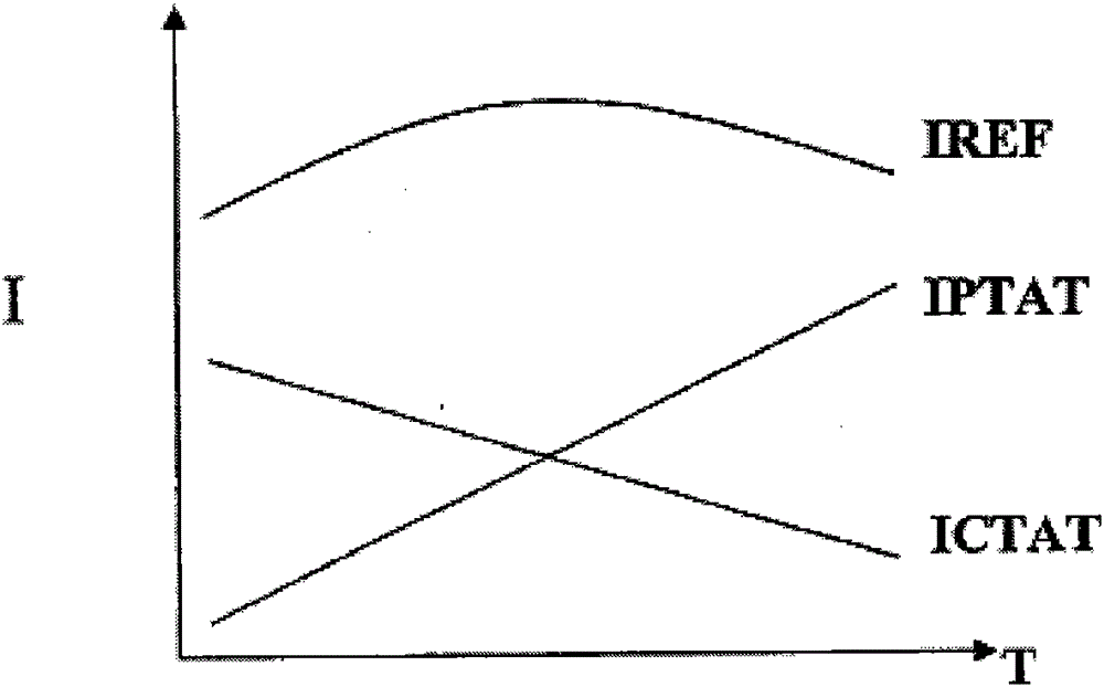
[0036] Embodiments of the present application described in detail now provide new methods and apparatus that provide temperature and process compensated bandgap reference circuits without adjustments.

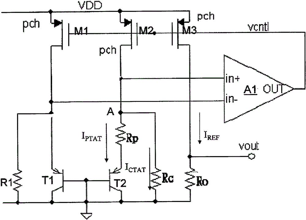
[0037] In an embodiment, the bandgap reference circuit is compensated by connecting two semiconductor devices each having a bandgap reference circuit, and thus the combined bandgap circuit output is compensated in case devices with opposite temperature drift effects are selected. In an embodiment, stacked devices are connected. For example, stacking two integrated circ...


PUM


Abstract

Structure and methods for a compensated bandgap reference circuit. A first integrated circuit die having a first bandgap reference circuit with a non-zero temperature coefficient; and having a first output reference signal is provided, a second integrated circuit die having a second bandgap reference circuit with a non-zero temperature coefficient that is of opposite polarity from the temperature coefficient of the first bandgap reference circuit, and having a second output reference signal is provided; an adder circuit disposed on at least one of the first and second integrated circuit dies combines the first and second output reference signals, and outputs a combined reference signal; and connectors for connecting the first and second output signals to the adder circuit are provided. Methods are disclosed for pairing integrated circuit dies with bandgap reference circuits and coupling the dies to form temperature compensated signals.

Description

technical field [0001] The field relates to the field of electronic circuits, and more particularly, to bandgap reference devices and methods. Background technique [0002] A common requirement for advanced electronic circuits and especially for circuits fabricated as integrated circuits ("ICs") in semiconductor manufacturing processes is the use of bandgap reference circuits. A bandgap reference circuit provides a current reference, or a voltage reference, for ideal temperature and independent process variation. The bandgap reference is designed to have a zero temperature coefficient ("TC"). Bandgap reference circuits are an essential component in many analog and mixed-signal circuits where fixed voltage and current references are required. In order to ensure a high-precision reference through a bandgap reference circuit in an integrated circuit device fabricated in a semiconductor manufacturing process, a test measurement and device trimming procedure is generally perfor...

Claims


Application Information

Patent Timeline
Patent Type & Authority Patents(China)
IPC IPC(8): G05F1/567
CPCG05F3/30
Inventor 陈致嘉彭迈杉
Owner TAIWAN SEMICON MFG CO LTD
Learn More