Write-once read-many disc internal memory

An on-chip memory and latch technology, applied in the field of multi-read single-write on-chip memory, can solve the problems of area consumption and slow speed, and achieve the effect of saving clock cycles

Active Publication Date: 2012-07-25
INST OF SEMICONDUCTORS - CHINESE ACAD OF SCI
View PDF1 Cites 10 Cited by
  • Summary
  • Abstract
  • Description
  • Claims
  • Application Information

AI Technical Summary

Problems solved by technology

Latch arrays are usually smaller than register files when the storage capacity is not particularly small, but they are slower and cannot support simultaneous reading and writing of the same storage unit like registers
On the contrary, the storage unit of the register file is a single register, which consumes at least a larger area than the latch on the storage unit, which is also an important reason why the register file is no longer attractive when the capacity increases

Method used


Image

  • Write-once read-many disc internal memory
  • Write-once read-many disc internal memory
  • Write-once read-many disc internal memory

Examples


Embodiment 1

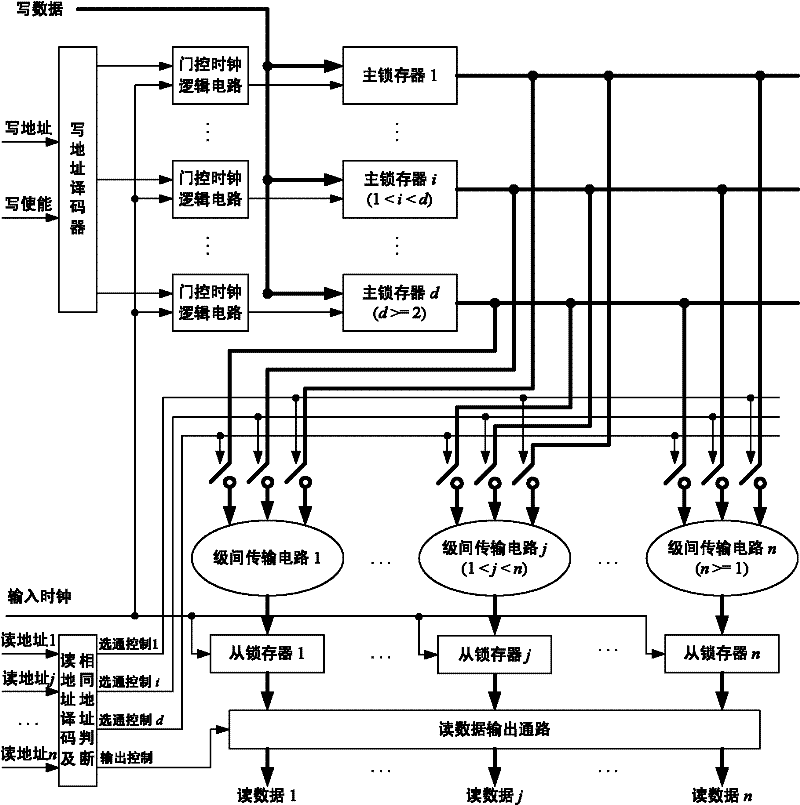
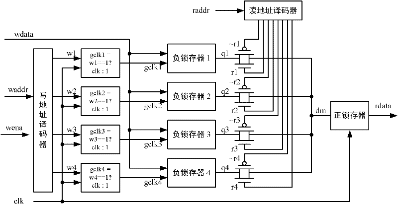
[0048] One embodiment is a 1R1W dual-port memory with a data port bit width of 1-bit and a storage capacity of 4 bits, as shown in the attached figure 2 shown.

[0049] The input and output ports of the memory are as follows:

[0050] port name

port direction

port width

port description

clk

input

1

Memory input clock signal

wena

input

1

memory write enable signal

waddr

input

2

memory write address

wdata

input

1

memory write data

raddr

input

2

memory read address

rdata

output

1

memory read data

[0051] The first level of the memory includes a write address decoder, 4 gating clock circuits, and 4 negative latches. The input of the write address decoder is clk, wena and waddr, and generates 4 decoded address control output signals w1, w2, w3, w4 synchronized with the rising edge of clk. Its logical relationship is shown in t...

Embodiment 2

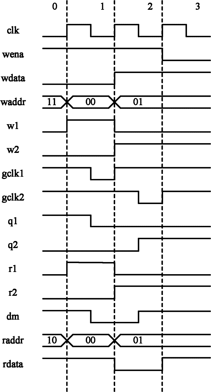
[0070] The only difference between Embodiment 2 and Embodiment 1 is: the output r1, r2, r3, r4 of the read address decoder and their opposite signals ~r1, ~r2, ~r3, ~r4 are synchronized with the falling edge of clk. Therefore, only the timing of reading data is changed. attached Figure 4 The timing diagram is given, taking r1 and r2 as examples, the process of reading data is:

[0071] Clock cycle 0: raddr selects negative latch 3, and rdata is the value 1 stored in negative latch 3.

[0072] Clock cycle 1: raddr changes on the falling edge of the clock cycle, selecting negative latch 1. Then r1=1, dm=q1. However, the positive latch is already in the latched state, and the value of rdata is still the value 1 corresponding to the previous negative latch 3.

[0073] Clock cycle 2: After the rising edge arrives, the positive latch starts to sample dm, at this time rdata=q1. raddr changes on the falling edge of the clock cycle, selecting negative latch 2. Then r2=1, dm=q2. ...

Embodiment 3

[0076] This embodiment is a 2R1W multi-port memory with a data port bit width of 1-bit and a storage capacity of 4 bits, see appendix Figure 5 .

[0077] Compared with Embodiment 1, the first stage of this embodiment is exactly the same as that of Embodiment 1. The difference is:

[0078] There are two sets of interstage transfer circuits and positive latches. Each group of inter-stage transmission circuits, positive latches, and their connection relationship with the first stage are the same, and are equivalent to Embodiment 1.

[0079] The read address decoding and identical address judgment module needs to decode two read address inputs raddr1 and raddr2 to generate strobe signals r1_1, r1_2, r1_3, r1_4, r2_1, r2_2, r2_3, r2_4 and their opposite signals. When raddr1 and raddr2 are different, the logical relationship between raddr1 and r1_1, r1_2, r1_3, r1_4 is the same as the logical relationship between raddr2 and r2_1, r2_2, r2_3, r2_4, and is equivalent to raddr and ...


PUM


Abstract

The invention discloses a write-once read-many disc internal memory, comprising a write address decoder, d (d>1) gate clock logic circuits, d first level main latches, n d input inter-stage transmission circuits, n second-level sub latches, a read data output path, and a read address decoding and same address judging module, wherein if the d first-level main latches are negative latches, the n second-level sub latches are positive latches; and if the d first-level main latches are positive latches, the n second-level sub latches are negative latches. The area of the memory unit close to the latches is realized, simultaneously the reading and writing features of the file in a register are held, that is, the same memory unit can be accessed by any reading port and any writing port in a same clock period.

Description

technical field [0001] The invention relates to the technical field of integrated circuit design, in particular to a multi-read single-write on-chip memory. Background technique [0002] In large-scale integrated circuit design, almost all chips have on-chip memory to provide fast-access on-chip data storage space. The two most important elements of on-chip memory are speed and cost (area). Common on-chip memories include SRAM, latch arrays, and register files. According to the consideration of speed and cost, with the reduction of storage capacity, the memory adopted is SRAM, latch array and register file in turn. [0003] In the data path, a large amount of small-capacity cache memory is usually required, and the small-capacity cache memory is generally implemented by a latch array or a register file. Such as the register file in the CPU. These cache memories generally support multi-port read and write, especially the one-read-one-write (1R1W) dual-port type. [0004]...

Claims


Application Information

Patent Timeline
Patent Type & Authority Applications(China)
IPC IPC(8): G11C7/22G11C8/00
Inventor 妙维吴南健
Owner INST OF SEMICONDUCTORS - CHINESE ACAD OF SCI
Why Eureka
Try Eureka