Field emission display structure by utilizing thick film medium as separant
A display structure and field emission technology, which is applied in the manufacture of image/graphic display tubes, discharge tubes/lamps, cathode ray tubes/electron beam tubes, etc. Inaccurate alignment and other problems, to avoid complex installation process, reduce process difficulty, and solve the effect of inaccurate alignment
- Summary
- Abstract
- Description
- Claims
- Application Information
AI Technical Summary
Problems solved by technology
Method used
Image
Examples
Embodiment 1
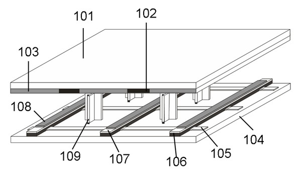
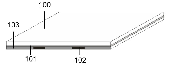
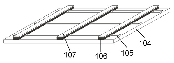
[0028] figure 1 It is a schematic diagram of a field emission display structure using thick-film dielectrics as spacers according to the first preferred embodiment of the present invention. Figure 2 to Figure 10 Schematically shows a structural diagram of a field emission display structure using thick film dielectrics as spacers. Combine the following Figure 2 to Figure 10 A field emission display structure using a thick-film dielectric as a spacer and a manufacturing method thereof provided in the first embodiment of the present invention will be described in detail.
[0029] A field emission display structure using a thick-film dielectric as a spacer and a manufacturing method thereof, characterized in that the field emission display structure is composed of a cathode substrate and an anode substrate, and a thick film is arranged between the cathode substrate and the anode substrate. The membrane dielectric spacer is arranged on the glass substrate of the cathode substra...
Embodiment 2
[0047] Figure 11 It is a schematic diagram of the structure of a field emission display using thick-film dielectrics as spacers according to the second embodiment of the present invention. The field emission display structure is composed of a cathode substrate and an anode substrate, a thick-film dielectric spacer is arranged between the cathode substrate and the anode substrate, the spacer is arranged on the glass substrate of the cathode substrate, and is firmly bonded to the glass substrate into a whole. The field emission display structure has a dipole structure, a triode structure and a multipole structure, and the triode structure or the multilevel structure includes a front gate structure, a rear gate structure and a flat gate structure, and the preferred second embodiment of the present invention provides A method for fabricating a gate-last type field emission display structure using a thick-film dielectric as an spacer, comprising the following steps:
[0048] s...
PUM
| Property | Measurement | Unit |
|---|---|---|
| Height | aaaaa | aaaaa |
| Surface diameter | aaaaa | aaaaa |
| Upper surface diameter | aaaaa | aaaaa |
Abstract
Description
Claims
Application Information


