Light-emitting diode (LED), backlight module and liquid crystal display device

A consistent, inner-cavity technology, applied to lighting devices, components of lighting devices, optics, etc., can solve problems such as unfavorable light dispersion, achieve the effects of increasing contact area, reducing electrode oxidation, and expanding the output angle

Inactive Publication Date: 2012-08-01
TCL CHINA STAR OPTOELECTRONICS TECH CO LTD
View PDF4 Cites 4 Cited by
  • Summary
  • Abstract
  • Description
  • Claims
  • Application Information

AI Technical Summary

Problems solved by technology

Common LED chip sink hole placement is not conducive to the dispersion of light

Method used


Image

  • Light-emitting diode (LED), backlight module and liquid crystal display device
  • Light-emitting diode (LED), backlight module and liquid crystal display device
  • Light-emitting diode (LED), backlight module and liquid crystal display device

Examples


Embodiment 1

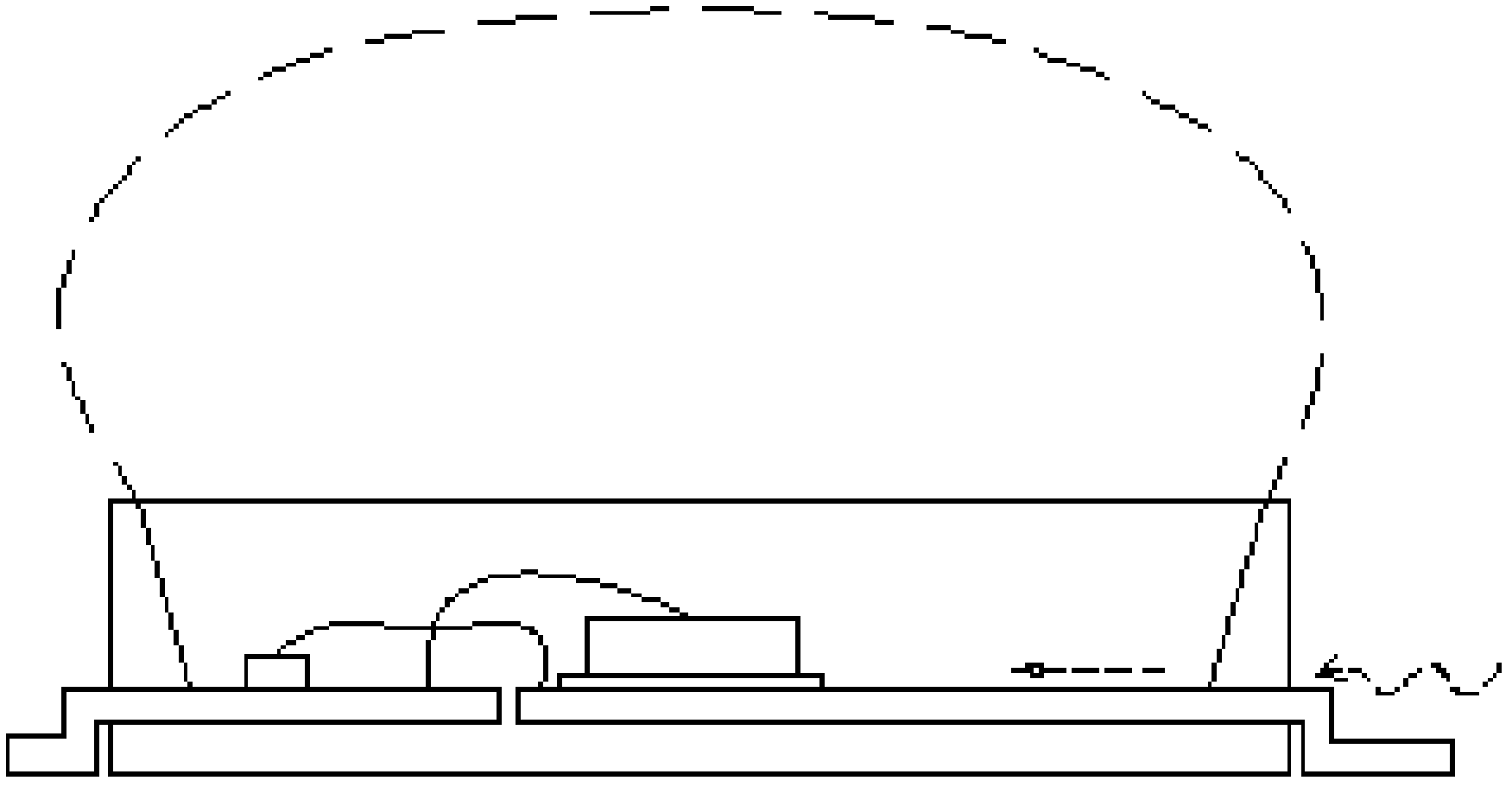
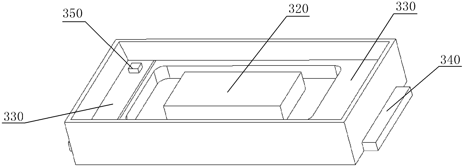
[0033] Such as Figure 6 As shown, one of the two side walls adjacent to the stepped surface is provided with a first slope 310, and the acute angle angle between the first slope 310 and the bottom plane of the inner cavity is in the range of 0.5° to 89°, Preferably, it is 30° to 60°. The electrodes 330 may be disposed on the two short side walls of the inner chamber, and correspondingly, the first slope 310 is disposed on the long side walls of the inner chamber. Certainly, the electrodes 330 may also be disposed on the two long side walls of the inner chamber, and correspondingly, the first slope 310 is disposed on the short side walls of the inner chamber.

[0034] In order to prevent the chip from being broken down by static electricity, a zener tube can be connected in series on one of the electrodes, and the zener tube is arranged on the step surface, which can prevent the zener tube from absorbing light.

Embodiment 2

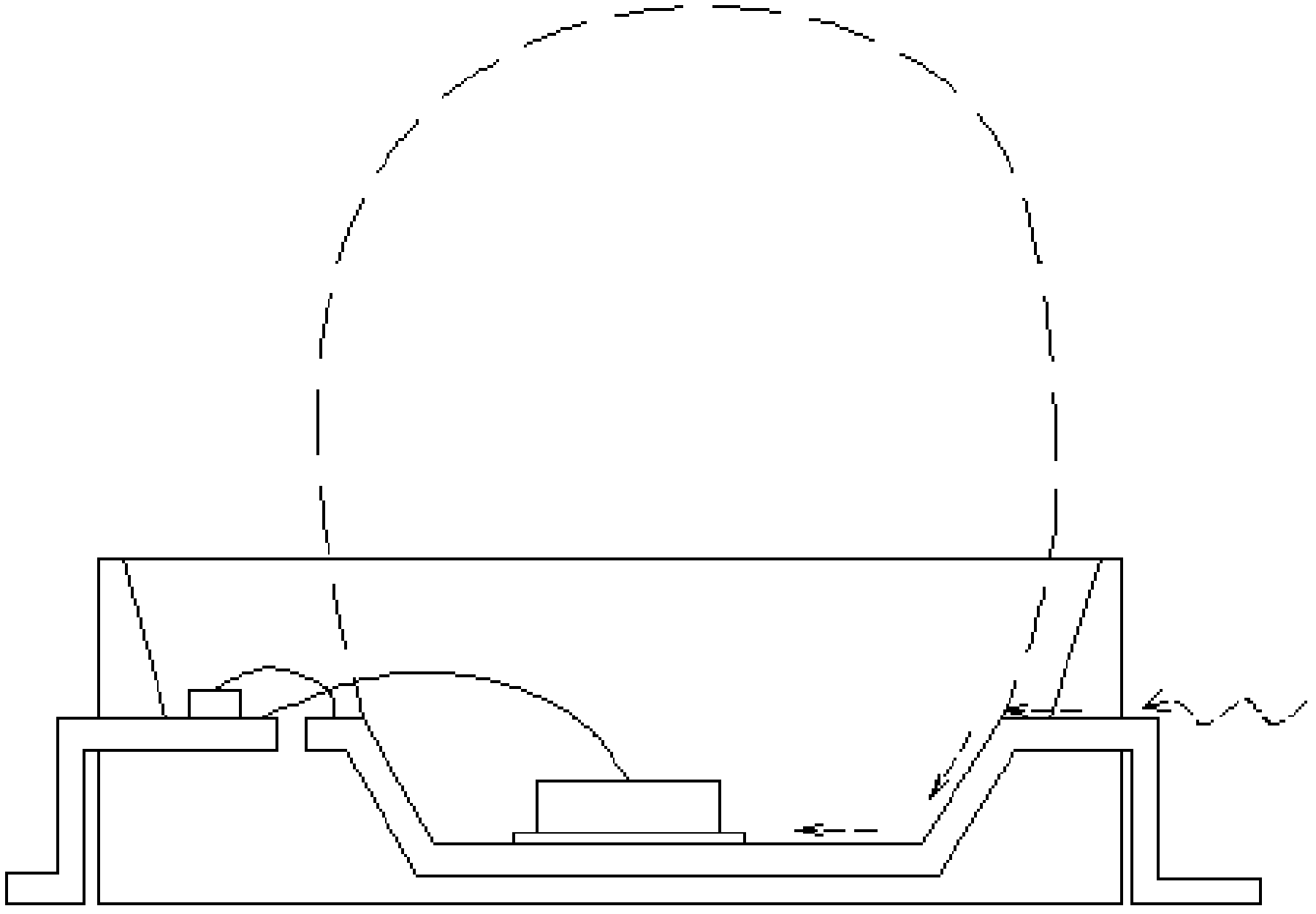
[0036] Such as Figure 7 As shown, the two side walls adjacent to the step surface are provided with slopes, which are the first slope 310 and the second slope 311 respectively, and the acute angle angle between the slope and the inner cavity bottom plane is in the range of 0.5° to 89° Between, preferably, 30° to 60°. The electrodes 330 may be disposed on two short side walls of the inner chamber, and correspondingly, the first slope 310 and the second slope 311 are disposed on the long side walls of the inner chamber. Certainly, the electrodes 330 may also be arranged on the two long side walls of the inner cavity, and correspondingly, the first inclined surface 310 and the second inclined surface 311 are arranged on the short side walls of the inner cavity.

[0037] In order to prevent the chip from being broken down by static electricity, a zener tube can be connected in series on one of the electrodes, and the zener tube is arranged on the step surface, which can prevent ...

Embodiment 3

[0039] Such as Figure 8 As shown, one electrode 330 provided with a zener tube 350 protrudes to form a stepped surface 331 at the bottom of the inner cavity, while the other electrode 330 is arranged at the bottom of the inner cavity, and the corresponding side of the inner cavity is also provided with a slope, A third slope 360 ​​is formed, and the acute angle between the slope and the bottom plane of the cavity is in the range of 0.5° to 89°, preferably 30° to 60°. This embodiment can be combined with any one of the first and second embodiments above, especially with the second embodiment, so that three of the four side walls of the inner cavity are provided with slopes to form a first The inclined surface 310, the second inclined surface 311, and the third inclined surface 360 ​​can ensure the maximum range of light emission.

[0040] The electrodes 330 are arranged on the two short side walls of the inner cavity, and correspondingly, the first inclined surface 310 and th...


PUM

PropertyMeasurementUnit
angleaaaaaaaaaa
angleaaaaaaaaaa

Abstract

The invention discloses a light-emitting diode (LED), a backlight module and a liquid crystal display device. The LED comprises a cavity, a chip is arranged at the bottom of the cavity, four lateral wall surround the bottom of the cavity, two ends of the chip are connected with electrodes, at least one protruded step face is arranged at the positions of two of the opposite lateral walls at the bottom of the cavity, and the electrodes at two ends of the chip extend to the step face from the bottom of the cavity. At least one of the other two lateral walls adjacent to the step face is provided with an inclined face forming an obtuse angle with the bottom of the cavity. The LED can flexibly control scattering range of emergent rays by selecting different included angles of the inclined face, is strong in adaptability and especially suitable for serving as a backlight source of the liquid crystal display device. When light enters in side mode, large emergent angles can enable rays to be evenly emitted into a light guide plate so as to reduce the phenomenon of hot spots.

Description

technical field [0001] The invention relates to the field of electronic display, and more specifically relates to an LED, a backlight module and a liquid crystal display device. Background technique [0002] Light-emitting diodes (LEDs) have been widely used in fields such as display and illumination due to their small size and high light efficiency. In liquid crystal display devices, LEDs have also begun to be used as backlight sources for liquid crystal displays. [0003] LED common structure such as figure 1 As shown, the chip is fixed on the electrode with silver glue. Since the electrode is made of metal, the LED frame is made of plastic or ceramic material. The top of the electrode is usually filled with potting glue such as epoxy resin or silica gel. The expansion rates of these materials are different. , so there are cracks at the joint between the plastic and the electrode and the joint between the potting glue and the electrode, and the crack will grow along the e...

Claims


Application Information

Patent Timeline
Patent Type & Authority Applications(China)
IPC IPC(8): H01L33/48F21V19/00G02F1/13357
CPCH01L33/60G02F1/133603H01L2224/48091G02F1/133615F21V19/00H01L33/486
Inventor 萧宇均唐国富
Owner TCL CHINA STAR OPTOELECTRONICS TECH CO LTD
Why Eureka
Try Eureka