Method for manufacturing X-ray sensor

A manufacturing method and sensor technology, applied in radiation control devices, electric solid devices, semiconductor devices, etc., can solve problems such as low yield rate, high product cost, and excessive mask exposure times

Active Publication Date: 2012-08-08
BEIJING BOE OPTOELECTRONCIS TECH CO LTD
View PDF4 Cites 13 Cited by
  • Summary
  • Abstract
  • Description
  • Claims
  • Application Information

AI Technical Summary

Problems solved by technology

[0007] The embodiment of the present invention provides a method for manufacturing an X-ray sensor, which is used to solve the problems of high product cost, low yield rate and equipment capacity caused by too many mask exposure times in the process of manufacturing an X-ray sensor in the prior art. low problem

Method used


Image

  • Method for manufacturing X-ray sensor
  • Method for manufacturing X-ray sensor
  • Method for manufacturing X-ray sensor

Examples


Embodiment Construction

[0036] Aiming at the problems of high product cost, low yield rate and low equipment productivity caused by too many mask exposure times in the process of manufacturing X-ray sensors in the prior art, an embodiment of the present invention provides an X-ray sensor and its production method.

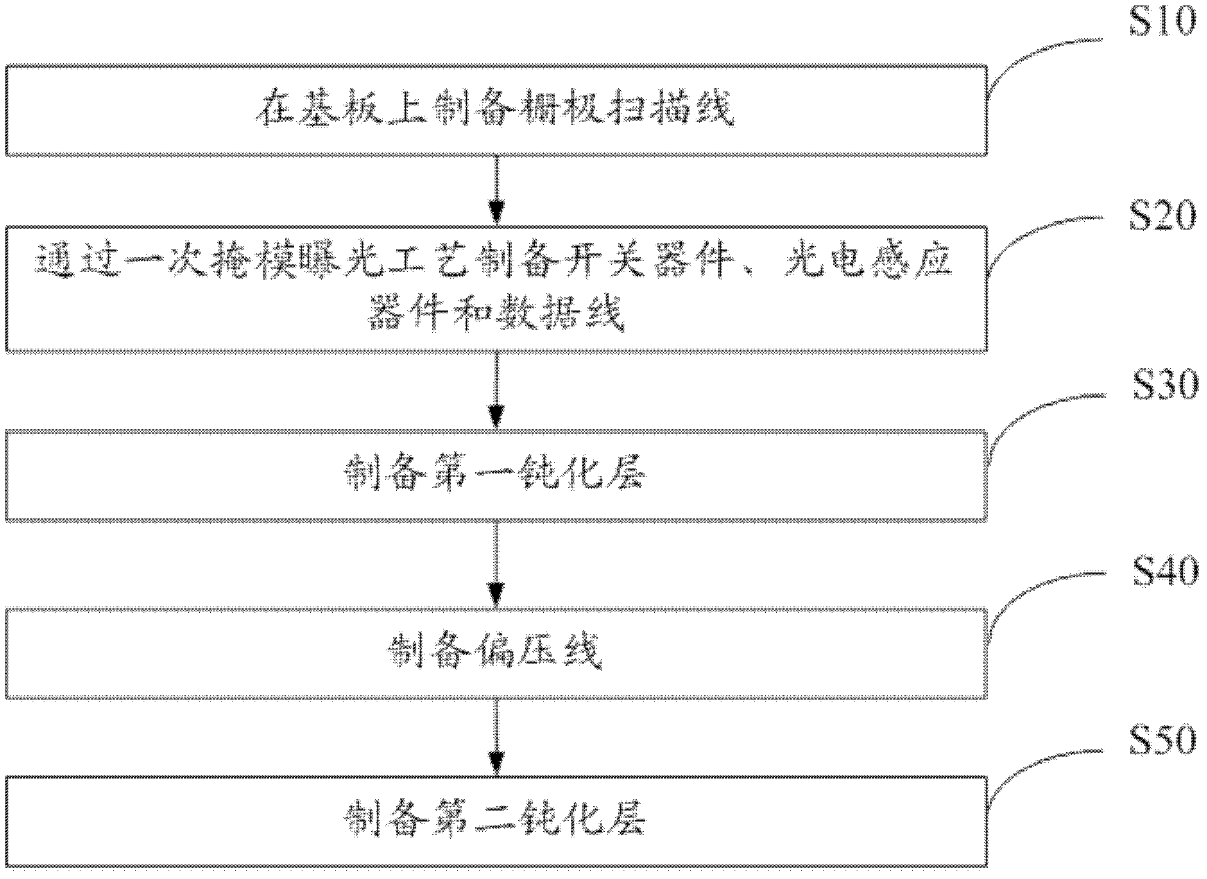
[0037] The manufacturing method of the X-ray sensor provided by the embodiment of the present invention, its process is as follows image 3 shown, including the following steps:

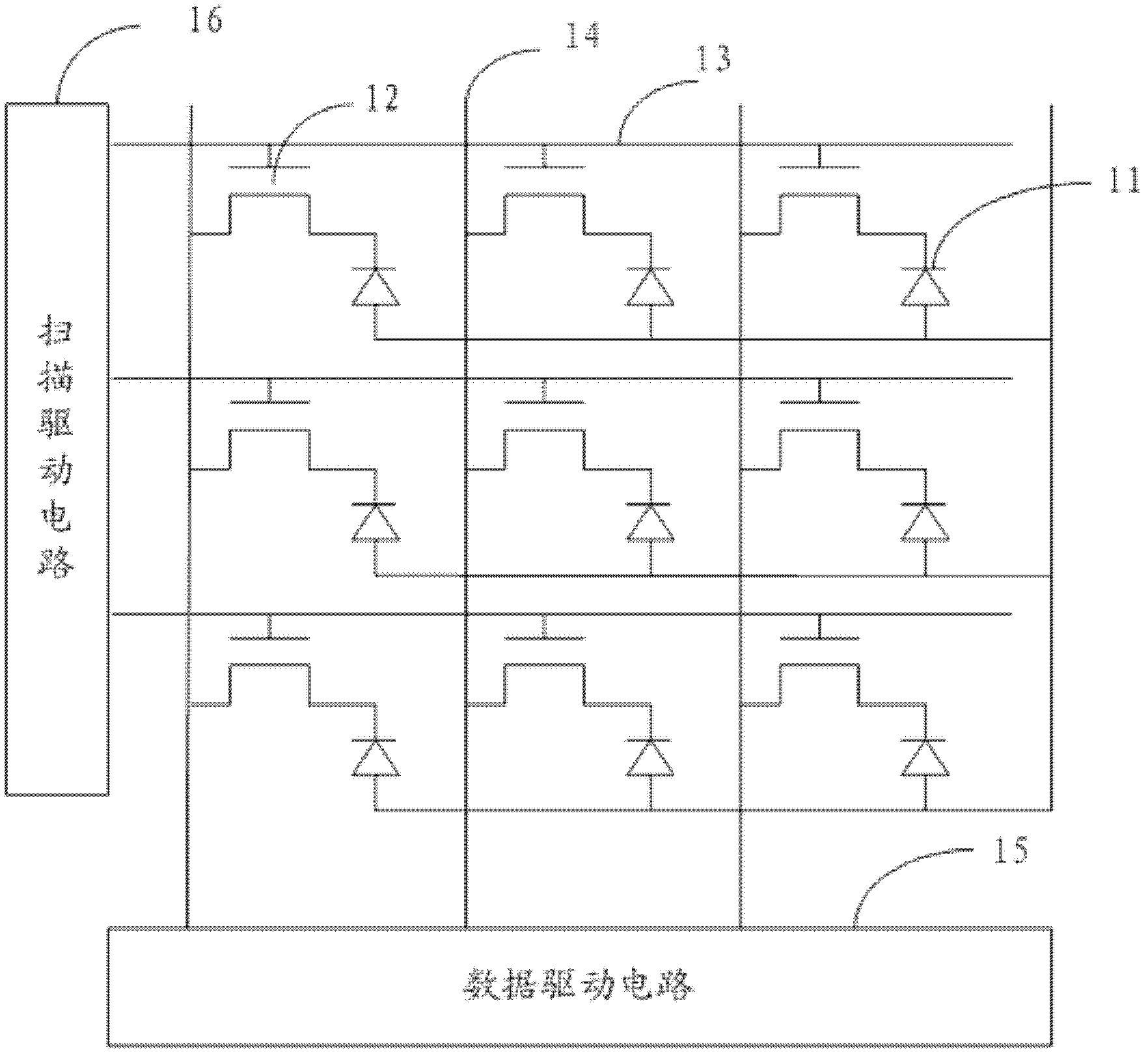
[0038] Step S10: preparing at least two gate scanning lines on the substrate; each gate scanning line serves as a gate of a switching device included in a row of pixel units in the X-ray sensor.

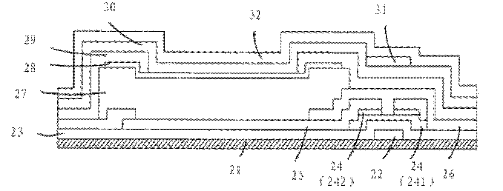
[0039] Step S20: sequentially depositing a gate insulating layer, an active layer film, an ohmic contact layer film, a first conductive layer film, and a photoelectric conversion layer film on the substrate and the gate scanning line; for the active layer film, the ohmic contact layer film, the second A conductive la...


PUM


Abstract

The invention discloses a method for manufacturing an X-ray sensor. The method comprises: preparing at least two gate scanning lines on a substrate; successively depositing a gate insulation layer, an active layer film, an ohmic contact layer film, a first conducting layer film, and a photovoltaic conversion layer film on the substrate and the gate scanning line and preparing at least two data lines intersected with the gate scanning lines, a photoelectric sensing device and a switching device; preparing a first passiviation layer covering the photoelectric sensing device and the switching device and preparing a via hole on the first passiviation layer, wherein the via hole is located at a selected position in a photoelectric sensing device region; preparing bias lines at a positions corresponding to positions of the data lines and the switching device on the first passiviation layer, wherein the bias lines are electrically connected with the photoelectric sensing device through the via hole; and preparing a second passiviation layer covering the bias lines and the first passiviation layer. According to the method provided by the invention, product cost is reduced and a yield rate and equipment capacity are improved.

Description

technical field [0001] The invention relates to the field of semiconductor devices, in particular to a manufacturing method of an X-ray sensor. Background technique [0002] With the development of society and the continuous advancement of science and technology, X-ray sensors not only play a very important role in the field of medical imaging, but also have been widely used in other fields such as metal flaw detection. [0003] The structure of the flat-panel X-ray sensor is similar to that of the liquid crystal display, such as figure 1 As shown, each pixel unit of the X-ray sensor includes a photodiode 11 and a thin film transistor (Thin Film Transistor, TFT) 12, the gate of TFT12 is connected with the grid scanning line 13 of the X-ray sensor, and the drain of FET12 It is connected to the data line 14 of the X-ray sensor, the source of the TFT 12 is connected to the photodiode 11, and one end of the data line 14 is connected to the data driving circuit 15 through a conn...

Claims


Application Information

Patent Timeline
Patent Type & Authority Applications(China)
IPC IPC(8): H01L27/146
CPCH01L27/144H01L27/14683
Inventor 徐少颖谢振宇陈旭
Owner BEIJING BOE OPTOELECTRONCIS TECH CO LTD
Why Eureka
Try Eureka