Preparation method of memory

A memory and active device technology, which is applied in the field of split-gate flash memory memory and memory preparation, can solve the problems of increasing metal line density, manufacturing difficulties, unsuitable for popularization and promotion, etc., to reduce chip area and avoid over-erasing , Increase the effect of process steps and process difficulty

Active Publication Date: 2012-08-15
SHANGHAI HUAHONG GRACE SEMICON MFG CORP
View PDF3 Cites 17 Cited by
  • Summary
  • Abstract
  • Description
  • Claims
  • Application Information

AI Technical Summary

Problems solved by technology

Increasing the density of cells will increase the density of metal lines, which is difficult to manufacture because the required masking and etching steps will need to produce very fine line
Therefore, the scheme of increasing the density of memory cells by increasing the number of memory cells has very high requirements on the process, which is not suitable for popularization and promotion.

Method used


Image

  • Preparation method of memory
  • Preparation method of memory
  • Preparation method of memory

Examples


Embodiment Construction

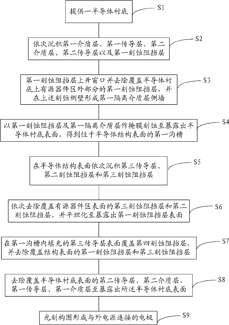
[0038] In order to make the object, technical solution and advantages of the present invention clearer, the present invention will be further described in detail below in conjunction with the accompanying drawings.

[0039] figure 1 The flow chart of the memory preparation method provided by the present invention.

[0040] like figure 1 As shown, the memory preparation method provided in this specific embodiment includes:

[0041] Step S1: providing a semiconductor substrate 100 .

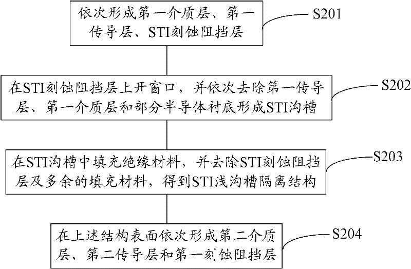
[0042] In this step, the semiconductor substrate is generally a silicon substrate or an SOI substrate. like Figure 4 As shown, the semiconductor substrate 100 has an active device region 010 and other device regions 020 thereon.

[0043] Step S2 : sequentially forming a first dielectric layer 101 , a first conductive layer 110 , a second dielectric layer 102 , a second conductive layer 120 and a first etch stop layer 111 on the semiconductor substrate 100 .

[0044] This step also includes t...


PUM


Abstract

The invention relates to a preparation method of a memory and belongs to the technical field of semiconductors. The preparation of a control grid and a floating grid of a memory bit unit and a memory word line is sequentially completed on a semiconductor substrate, in addition, the etching on a second coupling conducting layer is completed step by step, and the preparation of lead-out electrodes of other semiconductor devices on the substrate is completed under the condition of not influencing the structure of the memory. In the method, the chip area of a split grid flash memory is effectively reduced through the word line sharing memory under the condition of maintaining the electric isolation performance of the chip unchanged, and meanwhile, the over erasing problem can also be avoided. In addition, in the preparation method of the memory provided by the invention, the memory array word line and the lead-out electrodes of other semiconductor devices on the substrate are synchronously completed, any process steps and process difficulty are not added, and the semiconductor structures of the memory and the like cannot be damaged and influenced in the preparation process.

Description

technical field [0001] The invention relates to a method for preparing a memory, in particular to a method for preparing a split-gate flash memory, and belongs to the technical field of semiconductors. Background technique [0002] Flash memory has become a research hotspot in non-volatile memory due to its convenience, high storage density, and good reliability. Since the first flash memory product came out in the 1980s, with the development of technology and the storage needs of various electronic products, flash memory has been widely used in mobile and communication devices such as mobile phones, notebooks, handheld computers and U disks. , flash memory is a kind of non-volatile memory. Its operating principle is to control the switch of the gate channel by changing the critical voltage of the transistor or memory cell to achieve the purpose of storing data, so that the data stored in the memory will not be lost due to power interruption. Disappears, and flash memory is...

Claims


Application Information

Patent Timeline
Patent Type & Authority Applications(China)
IPC IPC(8): H01L21/8247H01L27/115
Inventor 顾靖孔蔚然张博
Owner SHANGHAI HUAHONG GRACE SEMICON MFG CORP
Why Eureka
Try Eureka